 Hello! now
 tms@lcdchip.com



Texas Instruments TPS7A2533DRVR
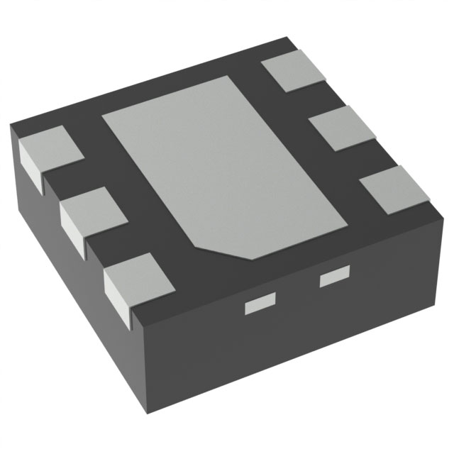
- Part No.:
- TPS7A2533DRVR
- Manufacturer:
- Texas Instruments
- Package:
- 6-WDFN Exposed Pad
- Description:
- IC REG LINEAR 3.3V 300MA 6WSON
- Quantity:
Unit Price:$0
Ext Price:$0
- Payment:

- Shipping:


Product Details
TPS7A2533DRVR - 3.3 V, 300 mA, 18 V Ultra-Low-IQ LDO
Texas Instruments TPS7A2533DRVR is the fixed 3.3 V member of the TPS7A25 low-dropout regulator family, combining 2 µA typical no-load ground current with enable and open-drain power-good functions.
The exact orderable, fixed-voltage pinout, package, carrier, quality record, and electrical limits were checked against TI-controlled product and data-sheet information.
Overview
This device regulates a 3.3 V rail from inputs up to 18 V and supplies loads through 300 mA. Its ultra-low standby demand, 1% output accuracy over temperature, internal soft start, and power-good output suit supervised low-power rails.
Key Advantages
2 µA typical ground current at no load supports long-duration battery and always-on applications.
The recommended input range extends from 2.4 V to 18 V.
An open-drain PG output provides a logic indication after the 3.3 V rail reaches its valid region.
Enable, UVLO, and internal soft start provide orderly turn-on behavior.
Feature Summary
Supports loads from 0 to 300 mA subject to dropout and thermal limits.
The 33 code selects the internally divided fixed-voltage version.
Fixed-output accuracy is specified to ±1% over the characterized temperature range.
210 mV typical and 340 mV maximum at 300 mA under the specified test conditions.
Includes overcurrent limiting, thermal shutdown, UVLO, and active overshoot pulldown.
Specified for -40°C to +125°C operating junction temperature.
Package & Footprint
TPS7A2533DRVR uses TI's DRV0006A package: a six-pin, 2.0 mm × 2.0 mm WSON with a central exposed pad and 0.8 mm maximum height. The catalog records the package under the generic name 6-WDFN Exposed Pad.
- Use TI drawing DRV0006A and its current land pattern.
- Verify pin-1 orientation and the no-lead footprint before PCB release.
- Connect the exposed pad to a large ground plane for best thermal performance.
- Place input and output ceramic capacitors close to the device pins and ground.
Pin Functions
The fixed-output DRV top view assigns pin 1 OUT, pin 2 NC, pin 3 PG, pin 4 EN, pin 5 GND, and pin 6 IN. The exposed thermal pad may be left floating, but TI recommends connecting it to a large ground plane for best thermal performance.
Regulated 3.3 V output; connect the stability capacitor to ground.
No internal connection; grounding can improve thermal performance.
Open-drain power-good output requiring an external pullup when used.
Active-high enable input; do not leave floating.
Ground and current-return connection.
Supply input and input-capacitor connection.
Thermal pad; connect to a broad ground plane for best heat transfer.
Key Specifications
| Output | 3.3 V fixed |
|---|---|
| Output current | 0 to 300 mA, subject to dropout and thermal limits |
| Recommended input range | 2.4 V to 18 V |
| Fixed-output accuracy | ±1% over temperature |
| Dropout at 300 mA | 210 mV typical, 340 mV maximum |
| Ground current | 2 µA typical at no load; 15 µA typical at 1 mA load |
| Output current limit | 325 mA minimum, 510 mA typical, 720 mA maximum at the stated condition |
| Input capacitor | 1 µF recommended minimum |
| Output capacitor | 1 µF to 100 µF nominal range; 2.2 µF nominal recommendation |
| Control and monitor | Active-high EN; open-drain PG |
| Protection | UVLO, overcurrent, thermal shutdown, active overshoot pulldown |
| Operating junction temperature | -40°C to +125°C |
| Thermal resistance | 73.3°C/W junction-to-ambient under TI's stated board condition |
| Package / carrier | WSON DRV, 6 pins plus exposed pad; 3000-unit large tape and reel |
| Device marking | 1WSP |
Replacement Considerations
No unconditional substitute is asserted. Match the fixed 3.3 V output, 300 mA capability, 18 V input rating, accuracy, dropout, enable thresholds, PG behavior, capacitor requirements, DRV footprint, exposed-pad connection, and thermal performance.
Do not substitute the adjustable TPS7A2501 by family name alone: its pin 2 is FB, while pin 2 is NC on this fixed version. No internal product link is included because no exact API-confirmed alternative was established.
Manufacturer Information
Texas Instruments lists TPS7A2533DRVR as active production. The order code identifies the TPS7A25 family, 3.3 V fixed output, DRV package, and large tape-and-reel carrier.
TI lists Catalog rating, RoHS and REACH compliance, NiPdAu lead finish, Level-1 MSL at 260°C peak reflow, device marking 1WSP, and 3000 units per reel.
Applications
Low standby demand supports always-on sensor and control nodes.
Wide input tolerance and PG monitoring suit supervised controller rails.
Low quiescent current helps extend battery operating time.
Provides a regulated 3.3 V support rail when thermal dissipation is qualified.
Quality & Authenticity
Verify the complete TPS7A2533DRVR code, 2 mm × 2 mm no-lead body, exposed pad, reel label, lot traceability, and device marking 1WSP.
A leaded six-pin package image is not representative of this device. Mechanical acceptance must follow TI's current DRV0006A drawing and quality records.
FAQ
Is TPS7A2533DRVR fixed or adjustable?
It is the fixed 3.3 V orderable. The adjustable TPS7A2501 uses a different function on pin 2.
Can it supply 300 mA?
Yes, when input headroom, output-capacitor stability, junction temperature, and exposed-pad thermal design are all satisfied.
What capacitor is required?
TI specifies at least 1 µF nominal at input and output and recommends 2.2 µF nominal at the output. Account for voltage and temperature derating.
Can PG be left unused?
Yes. TI permits PG to float or connect to ground when monitoring is not required.
Is the registered JPG suitable?
No. The current JPG shows a leaded package and conflicts with the required leadless WSON form, so it must be corrected before publication.
Engineering Notice
This summary supports evaluation but does not replace TI-controlled documentation. Confirm capacitor effective value, enable and PG interfaces, startup, dropout, reverse-current exposure, fault behavior, and thermal design over the complete operating envelope.
Solder the exposed pad to suitable copper, keep capacitor loops short, and limit junction temperature to the recommended range. Repeated thermal-shutdown operation is not a substitute for correct heat management.
TPS7A2533DRVR Information
- Specifications
- Tags
- Product attributes
- Attribute value
- Manufacturer:
- Texas Instruments
- Series:
- -
- Package/Case:
- 6-WDFN Exposed Pad
- Packaging:
- Tape & Reel (TR)
- Product Status:
- Active
- Output Configuration:
- Positive
- Output Type:
- Fixed
- Number of Regulators:
- 1
- Voltage - Input (Max):
- 18V
- Voltage - Output (Min/Fixed):
- 3.3V
- Voltage - Output (Max):
- -
- Voltage Dropout (Max):
- 0.21V @ 300mA
- Current - Output:
- 300mA
- Current - Quiescent (Iq):
- 4.5 µA
- Current - Supply (Max):
- -
- PSRR:
- 75dB ~ 52dB (10Hz ~ 1kHz)
- Control Features:
- Enable, Power Good
- Protection Features:
- Over Current, Over Temperature
- Operating Temperature:
- -40°C ~ 125°C (TJ)
- Grade:
- -
- Qualification:
- -
- Mounting Type:
- Surface Mount
- Supplier Device Package:
- 6-WSON (2x2)
- Include Parts
- Popular Search
The following parts include "TPS7A2533DRVR" in Silicon Labs TPS7A2533DRVR.
- Part Number
- Manufacturer
- Package
- Description
- MIC5504-1.8YM5-TR Microchip Technology SC-74A, SOT-753 IC REG LINEAR 1.8V 300MA SOT23-5
- MIC5504-3.3YM5-TR Microchip Technology SC-74A, SOT-753 IC REG LINEAR 3.3V 300MA SOT23-5
- MIC5365-3.0YC5-TR Microchip Technology 5-TSSOP, SC-70-5, SOT-353 IC REG LINEAR 3V 150MA SC70-5
- MIC5365-1.8YC5-TR Microchip Technology 5-TSSOP, SC-70-5, SOT-353 IC REG LINEAR 1.8V 150MA SC70-5
- MIC5365-2.5YC5-TR Microchip Technology 5-TSSOP, SC-70-5, SOT-353 IC REG LINEAR 2.5V 150MA SC70-5
- MIC5365-3.3YC5-TR Microchip Technology 5-TSSOP, SC-70-5, SOT-353 IC REG LINEAR 3.3V 150MA SC70-5
- MIC5365-3.3YD5-TR Microchip Technology SOT-23-5 Thin, TSOT-23-5 IC REG LIN 3.3V 150MA TSOT23-5
- MIC5317-3.3YM5-TR Microchip Technology SC-74A, SOT-753 IC REG LINEAR 3.3V 150MA SOT23-5
- TLV1117LV33DCYR Texas Instruments TO-261-4, TO-261AA IC REG LINEAR 3.3V 1A SOT223-4
- MIC5317-3.3YMT-TZ Microchip Technology 4-UDFN Exposed Pad IC REG LINEAR 3.3V 150MA 4DFN
The following parts are popular search parts in Test and Measurement.
Inventory:6,608
Please send an inquiry. Send us your inquiry, and we will respond immediately.


