 Hello! now
 tms@lcdchip.com



Analog Devices Inc. ADP1763ACPZ0.95-R7

- Part No.:
- ADP1763ACPZ0.95-R7
- Manufacturer:
- Analog Devices Inc.
- Package:
- 16-WFQFN Exposed Pad, CSP
- Description:
- IC REG LINEAR 0.95V 3A 16LFCSP
- Quantity:
Unit Price:$0
Ext Price:$0
- Payment:

- Shipping:


Product Details
ADP1763ACPZ0.95-R7 — Analog Devices 3 A low-noise LDO, fixed 0.95 V
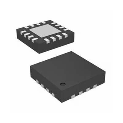
This exact ADP1763 order code is a fixed 0.95 V, 3 A low-dropout linear regulator supplied in a 16-lead, 3 mm by 3 mm LFCSP with exposed pad. It operates from a single 1.10 V to 1.98 V input and requires no auxiliary bias rail.
Overview
The ADP1763 family supplies low-voltage digital and sensitive mixed-signal rails. The ACPZ0.95-R7 ordering option is factory fixed at 0.95 V, with up to 3 A output current subject to input headroom and board thermal design. The R7 option is supplied on a 1,500-piece reel according to the manufacturer ordering guide.
Key Advantages
A single low-voltage input reduces power-tree complexity. Analog Devices reports 2 microvolts RMS output noise over 100 Hz to 100 kHz for the stated family test conditions and 95 mV typical dropout at 3 A for output voltages at least 1.2 V; the latter condition does not specify the 0.95 V option. Remote SENSE, soft start and power-good signaling help support demanding point-of-load designs.
Feature Summary
Integrated functions include enable control, an open-drain PG output, externally programmable soft start, current limit and thermal shutdown. The device is designed for stable operation with a 10 microfarad ceramic output capacitor. The fixed-voltage option leaves VADJ unconnected.
Package & Footprint
Original registered package: 16-WFQFN Exposed Pad, CSP. Analog Devices calls the exact part's package a 16-lead 3 mm by 3 mm LFCSP with exposed pad, outline CP-16-22. The package JPG is representative; use the CP-16-22 mechanical drawing for the PCB footprint and connect the exposed pad to the ground plane.
Pin Functions
| Pin | Name | Function |
|---|---|---|
| 1–4 | VIN | Connect all four to the input supply; bypass to ground with at least 10 microfarads. |
| 5 | REFCAP | Connect 1 microfarad to ground; do not load this pin. |
| 6 | VREG | Bypass to ground with at least 1 microfarad; do not load this pin. |
| 7 | GND | Ground. |
| 8 | VADJ | Leave floating for this fixed 0.95 V option. |
| 9–12 | VOUT | Connect all four to the load; bypass with at least 10 microfarads. |
| 13 | SENSE | Sense the output close to the load to reduce trace-drop error. |
| 14 | SS | Soft-start capacitor; 10 nF gives approximately 0.6 ms startup under stated conditions. |
| 15 | PG | Open-drain power-good output requiring an external pull-up. |
| 16 | EN | High enables; low disables. Tie to VIN for automatic startup. |
| EP | GND | Bottom exposed pad electrically connected to ground. |
Key Specifications
| Manufacturer | Analog Devices |
|---|---|
| Exact order code | ADP1763ACPZ0.95-R7 |
| Regulator type | Low-noise LDO linear regulator |
| Fixed output | 0.95 V nominal |
| Input range | 1.10 V to 1.98 V |
| Maximum output current | 3 A, subject to thermal and input limits |
| Output capacitor | At least 10 microfarads ceramic |
| Reference and VREG capacitors | 1 microfarad and at least 1 microfarad, respectively |
| Operating junction temperature | -40 to +125 degrees C |
| Package | 16-lead 3 mm by 3 mm LFCSP with exposed pad, CP-16-22 |
| Manufacturer package marking | LUQ |
Selection Guidance
Confirm that the input remains within 1.10 V to 1.98 V and provides adequate headroom for a regulated 0.95 V rail at the required load and temperature. Connect every VIN and VOUT pin, place all required ceramic capacitors close to the package, route SENSE to the load, and provide copper and vias for exposed-pad heat removal. Check the data sheet's load, capacitor, startup and thermal guidance in the final PCB design.
Manufacturer Information
Primary source: Analog Devices ADP1763 data sheet, Rev. E, including the electrical specifications, pin table, ordering guide and output-voltage options. See the official ADP1763 product page for the family overview.
Applications
Potential applications include FPGA and DSP core supplies, industrial and instrumentation power rails, and low-noise mixed-signal circuits where the 0.95 V output and 3 A rating meet the design requirements.
Quality & Authenticity
Check the complete ADP1763ACPZ0.95-R7 order code, LUQ package marking, CP-16-22 outline, pin-one orientation, exposed pad and traceability against Analog Devices documentation. The non-W order code should not be described as the automotive-qualified W variant.
FAQ
Is this output adjustable?
No. This order code is fixed at 0.95 V; leave VADJ floating.
Does it need a separate bias supply?
No. The family operates from one 1.10 V to 1.98 V input supply.
What is required at PG?
PG is open drain and requires an external pull-up to produce a logic-high indication.
Engineering Notice
Use the current manufacturer data sheet for complete electrical limits, capacitor selection, layout and thermal calculations. Family typical dropout and noise figures must be applied only under their stated test conditions. The package JPG is illustrative.
ADP1763ACPZ0.95-R7 Information
- Specifications
- Tags
- Product attributes
- Attribute value
- Manufacturer:
- Analog Devices Inc.
- Series:
- -
- Package/Case:
- 16-WFQFN Exposed Pad, CSP
- Packaging:
- Tape & Reel (TR)
- Product Status:
- Active
- Output Configuration:
- Positive
- Output Type:
- Fixed
- Number of Regulators:
- 1
- Voltage - Input (Max):
- 1.98V
- Voltage - Output (Min/Fixed):
- 0.95V
- Voltage - Output (Max):
- -
- Voltage Dropout (Max):
- 0.145V @ 3A
- Current - Output:
- 3A
- Current - Quiescent (Iq):
- 8 mA
- Current - Supply (Max):
- 16 mA
- PSRR:
- 62dB ~ 33dB (10kHz ~ 1MHz)
- Control Features:
- Enable, Power Good, Soft Start
- Protection Features:
- Current Limit, Thermal Overload
- Operating Temperature:
- -40°C ~ 125°C (TJ)
- Grade:
- -
- Qualification:
- -
- Mounting Type:
- Surface Mount
- Supplier Device Package:
- 16-LFCSP (3x3)
- Include Parts
- Popular Search
The following parts include "ADP1763ACPZ0.95-R7" in Silicon Labs ADP1763ACPZ0.95-R7.
- Part Number
- Manufacturer
- Package
- Description
- MIC5504-1.8YM5-TR Microchip Technology SC-74A, SOT-753 IC REG LINEAR 1.8V 300MA SOT23-5
- MIC5504-3.3YM5-TR Microchip Technology SC-74A, SOT-753 IC REG LINEAR 3.3V 300MA SOT23-5
- MIC5365-3.0YC5-TR Microchip Technology 5-TSSOP, SC-70-5, SOT-353 IC REG LINEAR 3V 150MA SC70-5
- MIC5365-1.8YC5-TR Microchip Technology 5-TSSOP, SC-70-5, SOT-353 IC REG LINEAR 1.8V 150MA SC70-5
- MIC5365-2.5YC5-TR Microchip Technology 5-TSSOP, SC-70-5, SOT-353 IC REG LINEAR 2.5V 150MA SC70-5
- MIC5365-3.3YC5-TR Microchip Technology 5-TSSOP, SC-70-5, SOT-353 IC REG LINEAR 3.3V 150MA SC70-5
- MIC5365-3.3YD5-TR Microchip Technology SOT-23-5 Thin, TSOT-23-5 IC REG LIN 3.3V 150MA TSOT23-5
- MIC5317-3.3YM5-TR Microchip Technology SC-74A, SOT-753 IC REG LINEAR 3.3V 150MA SOT23-5
- TLV1117LV33DCYR Texas Instruments TO-261-4, TO-261AA IC REG LINEAR 3.3V 1A SOT223-4
- MIC5317-3.3YMT-TZ Microchip Technology 4-UDFN Exposed Pad IC REG LINEAR 3.3V 150MA 4DFN
The following parts are popular search parts in Test and Measurement.
Inventory:1,434
Please send an inquiry. Send us your inquiry, and we will respond immediately.


