 Hello! now
 tms@lcdchip.com



Analog Devices Inc. ADP7102ACPZ-3.0-R7

- Part No.:
- ADP7102ACPZ-3.0-R7
- Manufacturer:
- Analog Devices Inc.
- Package:
- 8-WFDFN Exposed Pad, CSP
- Description:
- IC REG LINEAR 3V 300MA 8LFCSP
- Quantity:
Unit Price:$0
Ext Price:$0
- Payment:

- Shipping:


Product Details
ADP7102ACPZ-3.0-R7 — Analog Devices 3.0 V low-noise LDO
ADP7102ACPZ-3.0-R7 is the fixed 3.0 V order option in the ADP7102 linear-regulator family. Its package and output code are verified against manufacturer documentation. Evaluate supply headroom, output loading and thermal design before use.
Overview
The ADP7102 operates from 3.3 to 20 V input and can provide up to 300 mA under the stated electrical and thermal conditions. This order code supplies 3.0 V nominal output. The official package is CP-8-5 eight-lead 3 x 3 mm LFCSP with exposed pad.
Key Advantages
Low dropout, low-noise operation, enable control, compact packaging and protection functions support local analog and mixed-signal rails. Typical noise and dropout values vary with loading and external components; use the data-sheet limits for design margins.
Feature Summary
This fixed-output CMOS LDO offers low noise, high supply rejection, programmable EN/UVLO, power-good indication, reverse-current protection, foldback current limit and thermal protection. Its 300 mA capability is subject to thermal design.
Package & Footprint
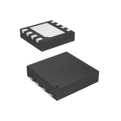
Original registered package: 8-WFDFN Exposed Pad, CSP. Manufacturer package: CP-8-5 eight-lead 3 x 3 mm LFCSP with exposed pad. The JPG is an illustrative package image, not a dimensional drawing. Follow the manufacturer's outline and recommended land pattern for assembly.
Pin Functions
| Pin | Name | Function |
|---|---|---|
| 1 | VOUT | Regulated output. |
| 2 | SENSE | Fixed-output remote-sense input; connect near the load. |
| 3, 6 and pad | GND | Ground; connect exposed pad to ground plane. |
| 4 | NC | Do not connect. |
| 5 | EN/UVLO | Enable and programmable undervoltage lockout. |
| 7 | PG | Open-drain power-good output; external pull-up if used. |
| 8 | VIN | Input supply. |
Key Specifications
| Manufacturer | Analog Devices |
|---|---|
| Exact model | ADP7102ACPZ-3.0-R7 |
| Fixed output | 3.0 V nominal |
| Rated output current | 300 mA under data-sheet conditions |
| Recommended input range | 3.3 to 20 V with output headroom |
| Output capacitor | 1 microfarad ceramic minimum under stated conditions |
| Operating junction range | -40 to +125 degrees C junction |
| Manufacturer package | CP-8-5 eight-lead 3 x 3 mm LFCSP with exposed pad |
Selection Guidance
Confirm 3.0 V rail tolerance, input range, worst-case dropout, load transient response, and board-level temperature at maximum load. Use at least 1 microfarad ceramic capacitors at VIN and VOUT, with effective capacitance checked under DC bias. Connect SENSE to the output near the load; connect the exposed pad to the ground plane and observe the 125 degrees C maximum operating junction temperature.
Manufacturer Information
Primary technical source: Analog Devices ADP7102 data sheet, Rev. E. The manufacturer product listing for ADP7102ACPZ-3.0-R7 confirms the exact order code and package. Review the latest electrical characteristics, pin table, output-capacitor conditions and mechanical drawing before production.
Applications
Suitable design contexts include noise-sensitive analog circuits, RF subsystems, data-converter rails and local point-of-load regulation where the specified voltage, current and thermal limits are satisfied.
Quality & Authenticity
Check the complete ADP7102ACPZ-3.0-R7 order code, package type, pin-one orientation and traceability against manufacturer documentation. Inspect the package and terminals before assembly.
FAQ
Is ADP7102ACPZ-3.0-R7 adjustable?
No. This order code is the fixed 3.0 V option.
What output capacitor is needed?
A 1 microfarad ceramic minimum is specified under the manufacturer's stated conditions; check effective capacitance and placement in the actual circuit.
How is SENSE connected?
For the fixed-output model, connect SENSE near the load to measure the regulated rail.
Engineering Notice
Follow the official data sheet for enable thresholds, absolute maximum ratings, capacitor placement and thermal derating. The 8-WFDFN-Exposed-Pad JPG is representative only. No live price or inventory claim is made.
ADP7102ACPZ-3.0-R7 Information
- Specifications
- Tags
- Product attributes
- Attribute value
- Manufacturer:
- Analog Devices Inc.
- Series:
- -
- Package/Case:
- 8-WFDFN Exposed Pad, CSP
- Packaging:
- Tape & Reel (TR)
- Product Status:
- Active
- Output Configuration:
- Positive
- Output Type:
- Fixed
- Number of Regulators:
- 1
- Voltage - Input (Max):
- 20V
- Voltage - Output (Min/Fixed):
- 3V
- Voltage - Output (Max):
- -
- Voltage Dropout (Max):
- 0.325V @ 300mA
- Current - Output:
- 300mA
- Current - Quiescent (Iq):
- 900 µA
- Current - Supply (Max):
- 1.4 mA
- PSRR:
- -
- Control Features:
- Enable, Power Good, Under Voltage Lockout
- Protection Features:
- Over Current, Over Temperature, Reverse Polarity
- Operating Temperature:
- -40°C ~ 125°C
- Grade:
- -
- Qualification:
- -
- Mounting Type:
- Surface Mount
- Supplier Device Package:
- 8-LFCSP-WD (3x3)
- Include Parts
- Popular Search
The following parts include "ADP7102ACPZ-3.0-R7" in Silicon Labs ADP7102ACPZ-3.0-R7.
- Part Number
- Manufacturer
- Package
- Description
- MIC5504-1.8YM5-TR Microchip Technology SC-74A, SOT-753 IC REG LINEAR 1.8V 300MA SOT23-5
- MIC5504-3.3YM5-TR Microchip Technology SC-74A, SOT-753 IC REG LINEAR 3.3V 300MA SOT23-5
- MIC5365-3.0YC5-TR Microchip Technology 5-TSSOP, SC-70-5, SOT-353 IC REG LINEAR 3V 150MA SC70-5
- MIC5365-1.8YC5-TR Microchip Technology 5-TSSOP, SC-70-5, SOT-353 IC REG LINEAR 1.8V 150MA SC70-5
- MIC5365-2.5YC5-TR Microchip Technology 5-TSSOP, SC-70-5, SOT-353 IC REG LINEAR 2.5V 150MA SC70-5
- MIC5365-3.3YC5-TR Microchip Technology 5-TSSOP, SC-70-5, SOT-353 IC REG LINEAR 3.3V 150MA SC70-5
- MIC5365-3.3YD5-TR Microchip Technology SOT-23-5 Thin, TSOT-23-5 IC REG LIN 3.3V 150MA TSOT23-5
- MIC5317-3.3YM5-TR Microchip Technology SC-74A, SOT-753 IC REG LINEAR 3.3V 150MA SOT23-5
- TLV1117LV33DCYR Texas Instruments TO-261-4, TO-261AA IC REG LINEAR 3.3V 1A SOT223-4
- MIC5317-3.3YMT-TZ Microchip Technology 4-UDFN Exposed Pad IC REG LINEAR 3.3V 150MA 4DFN
The following parts are popular search parts in Test and Measurement.
Inventory:1,502
Please send an inquiry. Send us your inquiry, and we will respond immediately.


