 Hello! now
 tms@lcdchip.com



onsemi NCP1117ST33T3G

- Part No.:
- NCP1117ST33T3G
- Manufacturer:
- onsemi
- Package:
- TO-261-4, TO-261AA
- Description:
- IC REG LINEAR 3.3V 1A SOT223
- Quantity:
Unit Price:$0
Ext Price:$0
- Payment:

- Shipping:


Product Details
NCP1117ST33T3G - 3.3 V, 1 A Low-Dropout Regulator
onsemi NCP1117ST33T3G is a fixed 3.3 V positive low-dropout regulator rated for output current above 1 A in Pb-free SOT-223, cataloged as TO-261-4 / TO-261AA.
Exact 3.3 V order code, limits, pinout, package, protection, capacitor requirements, temperature grade, and packing were verified against the onsemi NCP1117 controlled data sheet.
Overview
NCP1117ST33T3G provides a factory-set 3.3 V rail from a higher positive supply. It combines low-dropout regulation, current limiting, safe-operating-area compensation, and thermal shutdown in SOT-223.
Key Advantages
Fixed 3.3 V output
Factory-trimmed output eliminates an external programming divider.
High load capability
Output current exceeds 1 A when thermal and SOA limits permit.
Controlled dropout
Dropout is specified up to 1.20 V at 800 mA over temperature.
No minimum load
The fixed-output version is specified down to 0 mA load.
Feature Summary
Output accuracy
3.3 V is trimmed to plus or minus 1 percent at 25 degrees C under the stated condition.
20 V family operation
The family supports input up to 20 V, subject to each output option and dissipation limits.
Capacitor stability
A 4.7 microfarad minimum output capacitor within the specified ESR window is mandatory.
Integrated protection
Current limit, SOA compensation, and thermal shutdown are included.
Package & Footprint
The ST suffix identifies onsemi SOT-223 case 318H. TO-261-4 and TO-261AA are catalog aliases for this package family. The large tab and pin 2 are OUTPUT.
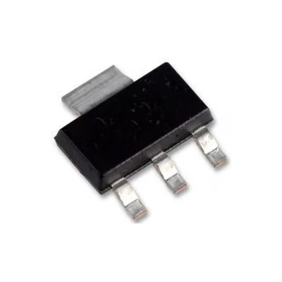
- Use onsemi case 318H dimensions and confirm top-view orientation.
- Connect the tab and pin 2 only to the 3.3 V output node.
- Provide output copper for current and heat spreading.
- Place input and output capacitors close to the regulator.
Registered local and production TO-261-4 JPGs matched; production returned HTTP 200 image/jpeg.
Pin Functions
The fixed 3.3 V SOT-223 top-view assignment is:
The tab is OUTPUT, not ground. Verify fixed-versus-adjustable pin 1 before reusing a footprint.
Key Specifications
| Manufacturer | onsemi |
|---|---|
| Function | Fixed 3.3 V positive low-dropout regulator |
| Output at 25 degrees C | 3.267 V minimum, 3.300 V typical, 3.333 V maximum at 5.3 V input and 10 mA |
| Output over line/load | 3.235 V minimum to 3.365 V maximum for 4.75 V to 10 V input and 0 mA to 800 mA |
| Output current | Above 1.0 A; do not exceed 1.0 A with VIN above 12 V |
| Dropout | 0.95 V typ / 1.10 V max at 100 mA; 1.01 V / 1.15 V at 500 mA; 1.07 V / 1.20 V at 800 mA |
| Current limit at 25 degrees C | 1.0 A minimum, 1.5 A typical, 2.2 A maximum at 5 V differential |
| Minimum load | 0 mA for fixed-output devices |
| Quiescent current | 6 mA typical, 10 mA maximum at 15 V input |
| Line regulation | 0.8 mV typical, 4.5 mV maximum for 4.75 V to 15 V input at 0 mA |
| Load regulation | 4.3 mV typical, 10 mV maximum from 0 mA to 800 mA at 4.75 V input |
| Ripple rejection | 60 dB minimum, 64 dB typical at 120 Hz under the stated condition |
| Output capacitor | 4.7 microfarads minimum; ESR typically 33 milliohms to 2.2 ohms |
| Operating ambient range | 0 degrees C to +125 degrees C |
| Package / packing | Pb-free SOT-223 case 318H; 4,000 units per tape and reel |
Typical values are not guaranteed limits. Apply all data-sheet test conditions, capacitor ESR limits, SOA guidance, and thermal derating.
Replacement Considerations
A replacement must match the fixed 3.3 V output, GROUND/OUTPUT/INPUT order, output-connected tab, current requirement, voltage limits, dropout, zero-load behavior, quiescent current, capacitor ESR window, protection, temperature grade, and SOT-223 mechanics. Adjustable and other fixed-voltage NCP1117 orderables are not direct functional substitutes.
No internal replacement link is asserted without an exact API-confirmed catalog record and engineering review.
Manufacturer Information
onsemi lists NCP1117ST33T3G as the 3.3 V NCP1117 in Pb-free SOT-223, supplied 4,000 units per tape and reel. The standard NCP grade is specified from 0 to +125 degrees C ambient and differs from NCP1117I and automotive NCV1117 variants.
Applications
3.3 V point-of-load rails
Local regulation in consumer and industrial equipment.
Post regulation
Final regulation after a switching converter.
Storage electronics
3.3 V rails for hard-drive controller circuitry.
General power conversion
Fixed low-noise rails with adequate input headroom and thermal design.
Quality & Authenticity
Verify the full NCP1117ST33T3G code, 3.3 V marking, case 318H dimensions, pin-1 orientation, reel label, Pb-free indicator, date code, and lot traceability. Appearance alone does not establish authenticity.
FAQ
Is the output adjustable?
No. This exact ST33 orderable is factory-set for 3.3 V.
Is a minimum load required?
No minimum load is specified for the fixed-output device.
Is the tab ground?
No. Pin 2 and the tab are OUTPUT.
What output capacitor is required?
At least 4.7 microfarads with ESR within the specified window.
Can it deliver 1 A continuously?
Only when dropout, SOA, PCB copper, ambient, and junction-temperature limits permit.
Engineering Notice
Use current onsemi controlled documents for final design. Confirm input range, dropout, capacitance and ESR across bias and temperature, transients, reverse discharge, SOA, thermal rise, and tab potential on the actual PCB.
NCP1117ST33T3G Information
- Specifications
- Tags
- Product attributes
- Attribute value
- Manufacturer:
- onsemi
- Series:
- -
- Package/Case:
- TO-261-4, TO-261AA
- Packaging:
- Tape & Reel (TR)
- Product Status:
- Active
- Output Configuration:
- Positive
- Output Type:
- Fixed
- Number of Regulators:
- 1
- Voltage - Input (Max):
- 20V
- Voltage - Output (Min/Fixed):
- 3.3V
- Voltage - Output (Max):
- -
- Voltage Dropout (Max):
- 1.2V @ 800mA
- Current - Output:
- 1A
- Current - Quiescent (Iq):
- 10 mA
- Current - Supply (Max):
- -
- PSRR:
- 64dB (120Hz)
- Control Features:
- -
- Protection Features:
- Over Current, Over Temperature
- Operating Temperature:
- 0°C ~ 125°C
- Grade:
- -
- Qualification:
- -
- Mounting Type:
- Surface Mount
- Supplier Device Package:
- SOT-223
- Include Parts
- Popular Search
The following parts include "NCP1117ST33T3G" in Silicon Labs NCP1117ST33T3G.
- Part Number
- Manufacturer
- Package
- Description
- MIC5504-1.8YM5-TR Microchip Technology SC-74A, SOT-753 IC REG LINEAR 1.8V 300MA SOT23-5
- MIC5504-3.3YM5-TR Microchip Technology SC-74A, SOT-753 IC REG LINEAR 3.3V 300MA SOT23-5
- MIC5365-3.0YC5-TR Microchip Technology 5-TSSOP, SC-70-5, SOT-353 IC REG LINEAR 3V 150MA SC70-5
- MIC5365-1.8YC5-TR Microchip Technology 5-TSSOP, SC-70-5, SOT-353 IC REG LINEAR 1.8V 150MA SC70-5
- MIC5365-2.5YC5-TR Microchip Technology 5-TSSOP, SC-70-5, SOT-353 IC REG LINEAR 2.5V 150MA SC70-5
- MIC5365-3.3YC5-TR Microchip Technology 5-TSSOP, SC-70-5, SOT-353 IC REG LINEAR 3.3V 150MA SC70-5
- MIC5365-3.3YD5-TR Microchip Technology SOT-23-5 Thin, TSOT-23-5 IC REG LIN 3.3V 150MA TSOT23-5
- MIC5317-3.3YM5-TR Microchip Technology SC-74A, SOT-753 IC REG LINEAR 3.3V 150MA SOT23-5
- TLV1117LV33DCYR Texas Instruments TO-261-4, TO-261AA IC REG LINEAR 3.3V 1A SOT223-4
- MIC5317-3.3YMT-TZ Microchip Technology 4-UDFN Exposed Pad IC REG LINEAR 3.3V 150MA 4DFN
The following parts are popular search parts in Test and Measurement.
Inventory:31,737
Please send an inquiry. Send us your inquiry, and we will respond immediately.


