 Hello! now
 tms@lcdchip.com



Texas Instruments LM5155DSSR
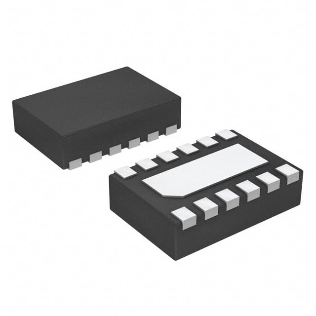
- Part No.:
- LM5155DSSR
- Manufacturer:
- Texas Instruments
- Category:
- DC DC Switching Controllers
- Package:
- 12-WFDFN Exposed Pad
- Description:
- POWER MANAGEMENT
- Quantity:
Unit Price:$1.66
Ext Price:$1.66
- Payment:

- Shipping:


Product Details
LM5155DSSR - Wide-Input Nonsynchronous Boost, SEPIC and Flyback Controller
LM5155DSSR from Texas Instruments is a peak current-mode DC/DC controller with a 1.5 A external MOSFET gate driver, a programmable 100 kHz to 2.2 MHz switching frequency, and support for boost, SEPIC, and flyback power stages.
The exact DSSR ordering code identifies the 12-pin WSON (DSS), 3 mm × 2 mm, large tape-and-reel option with 3,000 devices per reel.
Overview
The LM5155DSSR controls an external N-channel MOSFET in positive-output boost and SEPIC converters and in isolated or non-isolated flyback converters. Its wide BIAS range, low-current operating modes, programmable synchronization, adjustable soft start, power-good output, and protection functions support compact power supplies operating from batteries and industrial rails.
Key Advantages
A 3.5 V to 45 V operating range supports battery, industrial, and distributed-power inputs, with operation down to 1.5 V when BIAS is externally maintained.
Programmable operation up to 2.2 MHz can reduce magnetic and filter size when switching loss, EMI, and thermal limits permit.
The GATE output provides 1.5 A peak source or sink capability for a standard external N-channel MOSFET.
Programmable UVLO, cycle-by-cycle current limiting, OVP, thermal shutdown, soft start, slope compensation, synchronization, and PGOOD support robust system control.
Feature Summary
The CS input provides cycle-by-cycle peak current control with a 100 mV nominal threshold.
The controller accommodates step-up, step-up or step-down, and transformer-isolated power stages using an external MOSFET.
An RT resistor programs the switching frequency from 100 kHz to 2.2 MHz, and the UVLO/EN/SYNC input accepts external synchronization.
Typical operating quiescent current is approximately 450 µA, with shutdown current specified up to 2.6 µA.
Package & Footprint
LM5155DSSR is supplied in TI's 12-pin WSON (DSS) surface-mount package with an exposed thermal pad and a nominal 3 mm × 2 mm body. The customer package registry maps this orderable part to 12-WFDFN Exposed Pad. The DSSR carrier is a 3,000-piece large tape-and-reel.

- Use TI's current DSS package drawing and recommended land pattern for final pad geometry.
- Connect the exposed pad to AGND and a suitable ground copper area for heat spreading.
- Keep the GATE and current-sense paths short, and separate CS, FB, COMP, RT, and SS routing from switching nodes.
- Place BIAS and VCC bypass capacitors close to their pins with short returns to PGND.
The registered package JPG is currently missing and must be added before publication. Confirm pin-1 orientation, exposed-pad geometry, stencil design, and assembly rules against TI's latest mechanical drawing.
Pin Functions
The following mapping is for the TI 12-pin WSON DSS package, top view.
The UVLO/EN/SYNC pin must not float. When the function is unused, follow TI's specified connection to BIAS. Confirm all passive values and grounding paths in the current datasheet.
Key Specifications
| Orderable Part Number | LM5155DSSR |
|---|---|
| Manufacturer | Texas Instruments |
| Controller Type | Nonsynchronous peak current-mode DC/DC controller |
| Supported Topologies | Boost, SEPIC and flyback |
| Operating Input Range | 3.5 V to 45 V; operation down to 1.5 V requires BIAS ≥ 3.5 V |
| Startup Range with BIAS = VCC | 2.97 V to 16 V |
| Switching Frequency | Programmable from 100 kHz to 2.2 MHz |
| Maximum Duty Cycle | 93% |
| Gate-Driver Peak Current | 1.5 A source or sink |
| Current-Limit Threshold | 100 mV nominal, ±7% |
| Operating Quiescent Current | Approximately 450 µA typical; TI feature limit ≤480 µA |
| Operating Temperature | −40 °C to +125 °C |
| Package | 12-pin WSON (DSS), 3 mm × 2 mm, exposed pad |
| Standard Reel Quantity | 3,000 pieces |
Typical values, limits, and operating ranges may use different test conditions. Use the TI electrical-characteristics tables and design equations for guaranteed limits and worst-case calculations.
Replacement Considerations
Evaluate alternatives using the full ordering code. Package similarity does not by itself prove electrical or qualification equivalence.
- LM5155DSST: TI lists this as the same LM5155 device and DSS package in a 250-piece small tape-and-reel carrier. The electrical function and footprint are the closest match; confirm purchasing and carrier requirements.
- LM51551DSSR: Same controller family and 12-pin DSS package, with hiccup-mode overload protection enabled. Revalidate overload recovery, startup behavior, and system fault requirements.
- LM5155QDSSRQ1: Automotive-qualified LM5155 variant with wettable-flank package details and an operating range extending to 150 °C. Confirm the exact land pattern, qualification requirements, marking, and approved bill of materials.
- LM5155QDSSTQ1: Small-reel automotive ordering option. It changes both carrier quantity and qualification class, so procurement and assembly documentation must be reviewed.
For every substitution, compare the exact package drawing, pin configuration, current-limit behavior, hiccup option, reference and UVLO behavior, temperature rating, wettable-flank designation, and carrier quantity before approving the change.
Manufacturer Information
Texas Instruments lists LM5155DSSR as an active catalog device. The controlled sources used for this summary are the LM5155DSSR orderable-part page and the LM5155/LM51551 datasheet, document SNVSB75E.
- Exact ordering identity: LM5155DSSR, WSON DSS, 12 pins, large tape-and-reel.
- Qualification: Catalog grade. Do not infer AEC-Q100 qualification from the related LM5155-Q1 family.
- Assembly data: TI lists NiPdAu lead finish, MSL 1 at 260 °C peak reflow, and RoHS compliance for this orderable part.
Applications
Boost Converters
Step-up conversion from battery or industrial rails using an external MOSFET, diode, inductor, and current-sense network.
SEPIC Supplies
Positive-output conversion where the regulated output may be above or below the input voltage.
Flyback Power Supplies
Isolated or non-isolated flyback stages with primary-side regulation options and application-specific transformer design.
Battery and Industrial Power
Wide-input systems that require programmable UVLO, low shutdown current, synchronization, and an external power switch.
Quality & Authenticity
- Identity: verify the complete LM5155DSSR ordering code, DSS package, 1U4H device marking, reel label, and pin-1 orientation.
- Traceability: retain supplier, lot, date-code, and packaging records required by the purchasing specification.
- Handling: follow current TI guidance for ESD, moisture sensitivity, storage, reflow, and exposed-pad assembly.
- Inspection: compare package dimensions and markings with controlled manufacturer data rather than relying on product photographs alone.
FAQ
What is the difference between LM5155DSSR and LM5155DSST?
Can LM5155DSSR operate from a 1.5 V input?
Does LM5155DSSR include the power MOSFET?
When should LM51551DSSR be considered?
Engineering Notice
LM5155DSSR Information
- Specifications
- Tags
- Product attributes
- Attribute value
- Manufacturer:
- Texas Instruments
- Series:
- -
- Package/Case:
- 12-WFDFN Exposed Pad
- Packaging:
- Tape & Reel (TR)
- Product Status:
- Active
- Output Type:
- Transistor Driver
- Function:
- Step-Up, Step-Up/Step-Down
- Output Configuration:
- Positive
- Topology:
- Boost, Flyback, SEPIC
- Number of Outputs:
- 1
- Output Phases:
- 1
- Voltage - Supply (Vcc/Vdd):
- 2.97V ~ 45V
- Frequency - Switching:
- 100kHz ~ 2.2MHz
- Duty Cycle (Max):
- 93%
- Synchronous Rectifier:
- No
- Clock Sync:
- Yes
- Serial Interfaces:
- -
- Control Features:
- Soft Start
- Operating Temperature:
- -40°C ~ 125°C (TJ)
- Grade:
- -
- Qualification:
- -
- Mounting Type:
- Surface Mount
- Supplier Device Package:
- 12-WSON (3x2)
- Include Parts
- Popular Search
The following parts include "LM5155DSSR" in Silicon Labs LM5155DSSR.
- Part Number
- Manufacturer
- Package
- Description
- UCC28C45DR Texas Instruments 8-SOIC (0.154", 3.90mm Width) IC REG CTRLR MULT TOPOLOGY 8SOIC
- UCC28C40DR Texas Instruments 8-SOIC (0.154", 3.90mm Width) IC REG CTRLR MULT TOPOLOGY 8SOIC
- UCC28C43DR Texas Instruments 8-SOIC (0.154", 3.90mm Width) IC REG CTRLR MULT TOPOLOGY 8SOIC
- ZXSC410E6TA Diodes Incorporated SOT-23-6 IC REG CTRLR BOOST SOT23-6
- LM3524DMX/NOPB Texas Instruments 16-SOIC (0.154", 3.90mm Width) IC REG CTRLR BUCK/BOOST 16SOIC
- LM3489MMX/NOPB Texas Instruments 8-TSSOP, 8-MSOP (0.118", 3.00mm Width) IC REG CTRLR BUCK 8VSSOP
- MIC2102YML-TR Microchip Technology 16-VFQFN Exposed Pad IC REG CTRLR BUCK 16MLF
- LM5148RGYR Texas Instruments 24-VFQFN Exposed Pad 3.5-V TO 80-V, CURRENT MODE SYNC
- TL598CDR Texas Instruments 16-SOIC (0.154", 3.90mm Width) IC REG CTRLR MULT TOP 16SOIC
- LM5155DSSR Texas Instruments 12-WFDFN Exposed Pad POWER MANAGEMENT
The following parts are popular search parts in Test and Measurement.
Inventory:0
Please send an inquiry. Send us your inquiry, and we will respond immediately.
In Stock:0
| Qty. | Unit Price | Ext. Price |
| 1+ | $1.66 | $1.66 |
| 10+ | $1.23 | $12.30 |
| 25+ | $1.12 | $28.00 |
| 100+ | $1.00 | $100.00 |
| 250+ | $0.94 | $235.00 |
| 500+ | $0.91 | $455.00 |
| 3000+ | $0.85 | $2550.00 |
| 6000+ | $0.83 | $4980.00 |
| 9000+ | $0.82 | $7380.00 |


