 Hello! now
 tms@lcdchip.com



Analog Devices Inc. ADP3335ACPZ-3.3-R7

- Part No.:
- ADP3335ACPZ-3.3-R7
- Manufacturer:
- Analog Devices Inc.
- Package:
- 8-WFDFN Exposed Pad, CSP
- Description:
- IC REG LINEAR 3.3V 500MA 8LFCSP
- Quantity:
Unit Price:$0
Ext Price:$0
- Payment:

- Shipping:


Product Details
ADP3335ACPZ-3.3-R7 - Fixed 3.3 V, 500 mA LDO
The Analog Devices ADP3335ACPZ-3.3-R7 is a fixed 3.3 V, 500 mA low-dropout linear regulator in the catalog's 8-WFDFN Exposed Pad, CSP package. The manufacturer's exact ordering guide identifies an 8-lead 3 mm × 3 mm LFCSP_WD, package option CP-8-13.
Specifications, pin functions and package details follow the Analog Devices ADP3335 Rev. D data sheet and exact-model product listing.
Overview
The ADP3335 regulates a 3.3 V rail from a 2.6 V to 12 V rated input supply when sufficient VIN-to-VOUT headroom exists. It supports up to 500 mA with appropriate thermal design. ADI's anyCAP architecture is specified to remain stable with a 1 µF or larger output capacitor, including ceramic types. An active-low shutdown input provides output control, and NR supports optional noise reduction.
Key Advantages
Factory-set 3.3 V output; no external feedback divider is required.
1 µF output capacitor minimum with broad ESR tolerance, including MLCC.
200 mV typical at 500 mA under data sheet conditions.
An NR terminal allows additional output-noise reduction in suitable designs.
Feature Summary
500 mA continuous capability, subject to dissipation and thermal limits.
80 µA typical ground current at 0.1 mA output load under specified conditions.
SD is an active-low shutdown input; connect it to IN when shutdown is unused.
Internal current limiting and thermal overload protection.
Package & Footprint
The catalog package entry is 8-WFDFN Exposed Pad, CSP, registered under 8-WFDFN Exposed Pad. ADI's ordering guide calls the exact ACPZ-3.3-R7 option an 8-lead, 3 mm × 3 mm LFCSP_WD, CP-8-13, with branding L1K. Use the controlled manufacturer outline for board land dimensions.
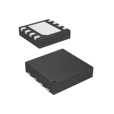
- Match package option CP-8-13 and the actual purchased part.
- The exposed pad is electrically common with IN; isolate thermal vias or connect them to IN. Never tie the pad to ground.
- Join all OUT terminals and both IN terminals as directed by the manufacturer.
The catalog JPG is illustrative and does not determine pinout or footprint. Package register image status needs review.
Pin Functions
ADI's ADP3335 8-lead LFCSP pin function table assigns:
Regulated output; connect all three pins and bypass to GND with at least 1 µF.
Ground terminal.
Noise-reduction terminal for optional output-noise reduction.
Active-low shutdown; ground disables output, connect to IN if unused.
Regulator input; connect both pins.
Electrically common with IN. Keep it isolated from GND.
Check the LFCSP top-view drawing and exposed-pad note rather than assuming another eight-pin regulator's layout.
Key Specifications
| Output voltage | 3.3 V fixed |
|---|---|
| Operating input rating | 2.6 V to 12 V, with headroom needed for 3.3 V regulation |
| Continuous output current | Up to 500 mA with thermal design |
| Dropout at 500 mA | 200 mV typical, 370 mV maximum under data sheet test conditions |
| Output voltage accuracy | ±0.9% at 25 °C over specified line/load conditions; ±1.8% over temperature conditions |
| Output capacitor | 1 µF or greater; ceramic supported |
| Ground current at 0.1 mA load | 80 µA typical, 110 µA maximum |
| Output noise | 47 µV rms typical, 10 Hz to 100 kHz, COUT = 10 µF and CNR = 10 nF at 500 mA |
| Shutdown control | Active low at SD |
| Operating ambient temperature | -40 °C to +85 °C |
| Package option | 8-lead 3 mm × 3 mm LFCSP_WD, CP-8-13 |
| Protection | Current limit and thermal overload protection |
Typical and maximum figures are separate. Calculate dropout headroom and junction temperature for the actual board.
Replacement Considerations
Other ADP3335 outputs such as 2.5 V or 5 V require a different rail specification. The adjustable ADP3334ACPZ family requires feedback resistors and has a different pinout and SD behavior, despite a similar CP-8-13 package. ADP3335 MSOP variants also differ mechanically. Compare full order code, exact pin map, exposed-pad net, output voltage, capacitor network, dropout, thermal performance and qualification before replacement. No unverified site alternative is linked or asserted as a drop-in substitute.
Manufacturer Information
Analog Devices lists ADP3335ACPZ-3.3-R7 as a production fixed 3.3 V model. The ADI ordering guide states 8-lead LFCSP_WD package option CP-8-13, -40 °C to +85 °C, and top branding L1K. Verify the full reel label and latest manufacturer documentation when ordering.
Applications
Compact fixed 3.3 V rails where a ceramic output capacitor is useful.
Local regulated logic supply up to the current and temperature limits.
Low-noise auxiliary rails when the NR and capacitor network are designed appropriately.
Board-level 3.3 V regulation with input headroom and thermal evaluation.
Quality & Authenticity
Confirm complete ADP3335ACPZ-3.3-R7 labeling, source traceability, CP-8-13 mechanical dimensions and expected L1K top branding. A package marking alone does not establish authenticity. Inspect the exposed-pad connection and assembly documentation.
FAQ
Is the output adjustable?
No. This exact -3.3-R7 order code is fixed at 3.3 V.
What is the SD polarity?
SD is active low for shutdown. Grounding SD disables the output; tie it to IN if shutdown is not used.
Can the exposed pad be grounded?
No. The manufacturer states that the LFCSP exposed pad is electrically common with IN and must not be tied to GND.
Does a 2.6 V input provide 3.3 V output?
No. The regulator needs sufficient input voltage above 3.3 V, including dropout and specified operating margin.
Engineering Notice
Use the latest ADI data sheet to verify effective capacitor value, NR wiring, SD control, input transients and thermal dissipation at worst-case load. Connect the LFCSP exposed pad to the appropriate input net or isolate its vias as directed, and review the final footprint and illustration before publication.
ADP3335ACPZ-3.3-R7 Information
- Specifications
- Tags
- Product attributes
- Attribute value
- Manufacturer:
- Analog Devices Inc.
- Series:
- anyCAP®
- Package/Case:
- 8-WFDFN Exposed Pad, CSP
- Packaging:
- Tape & Reel (TR)
- Product Status:
- Active
- Output Configuration:
- Positive
- Output Type:
- Fixed
- Number of Regulators:
- 1
- Voltage - Input (Max):
- 12V
- Voltage - Output (Min/Fixed):
- 3.3V
- Voltage - Output (Max):
- -
- Voltage Dropout (Max):
- 0.37V @ 500mA
- Current - Output:
- 500mA
- Current - Quiescent (Iq):
- 110 µA
- Current - Supply (Max):
- 10 mA
- PSRR:
- -
- Control Features:
- Shutdown
- Protection Features:
- Over Current, Over Temperature
- Operating Temperature:
- -40°C ~ 85°C (TA)
- Grade:
- -
- Qualification:
- -
- Mounting Type:
- Surface Mount
- Supplier Device Package:
- 8-LFCSP (3x3)
- Include Parts
- Popular Search
The following parts include "ADP3335ACPZ-3.3-R7" in Silicon Labs ADP3335ACPZ-3.3-R7.
- Part Number
- Manufacturer
- Package
- Description
- MIC5504-1.8YM5-TR Microchip Technology SC-74A, SOT-753 IC REG LINEAR 1.8V 300MA SOT23-5
- MIC5504-3.3YM5-TR Microchip Technology SC-74A, SOT-753 IC REG LINEAR 3.3V 300MA SOT23-5
- MIC5365-3.0YC5-TR Microchip Technology 5-TSSOP, SC-70-5, SOT-353 IC REG LINEAR 3V 150MA SC70-5
- MIC5365-1.8YC5-TR Microchip Technology 5-TSSOP, SC-70-5, SOT-353 IC REG LINEAR 1.8V 150MA SC70-5
- MIC5365-2.5YC5-TR Microchip Technology 5-TSSOP, SC-70-5, SOT-353 IC REG LINEAR 2.5V 150MA SC70-5
- MIC5365-3.3YC5-TR Microchip Technology 5-TSSOP, SC-70-5, SOT-353 IC REG LINEAR 3.3V 150MA SC70-5
- MIC5365-3.3YD5-TR Microchip Technology SOT-23-5 Thin, TSOT-23-5 IC REG LIN 3.3V 150MA TSOT23-5
- MIC5317-3.3YM5-TR Microchip Technology SC-74A, SOT-753 IC REG LINEAR 3.3V 150MA SOT23-5
- TLV1117LV33DCYR Texas Instruments TO-261-4, TO-261AA IC REG LINEAR 3.3V 1A SOT223-4
- MIC5317-3.3YMT-TZ Microchip Technology 4-UDFN Exposed Pad IC REG LINEAR 3.3V 150MA 4DFN
The following parts are popular search parts in Test and Measurement.
Inventory:658
Please send an inquiry. Send us your inquiry, and we will respond immediately.


