 Hello! now
 tms@lcdchip.com



onsemi LM317BD2TG

- Part No.:
- LM317BD2TG
- Manufacturer:
- onsemi
- Package:
- TO-263-3, D2PAK (2 Leads + Tab), TO-263AB
- Description:
- IC REG LIN POS ADJ 1.5A D2PAK-3
- Quantity:
Unit Price:$0
Ext Price:$0
- Payment:

- Shipping:


Product Details
LM317BD2TG - 1.2 V to 37 V Adjustable Positive Regulator
onsemi LM317BD2TG is an adjustable positive linear regulator capable of supplying more than 1.5 A in the surface-mount D2PAK-3 package.
The exact B-grade order code, -40 to 125 degrees C range, D2PAK pinout, electrical characteristics, Pb-free finish, and 50-unit rail packing were checked against the onsemi LM317 data sheet.
Overview
LM317BD2TG regulates a positive output from approximately 1.2 V to 37 V using an external resistor divider. It maintains a nominal 1.25 V reference between OUTPUT and ADJUST and integrates current limiting, thermal shutdown, and safe-operating-area compensation.
Key Advantages
Adjustable output
Two external resistors set outputs from about 1.2 V to 37 V.
More than 1.5 A capability
The pass stage supports high-current rails when differential voltage and thermal conditions permit.
Integrated protection
Current limiting, thermal shutdown, and safe-area compensation protect the regulator.
Extended temperature grade
The B-grade device is specified from -40 degrees C to 125 degrees C junction temperature.
Feature Summary
Floating operation
Regulation depends on input-to-output differential, enabling outputs at elevated potentials.
40 V differential rating
The absolute maximum input-to-output differential is 40 V.
Low adjustment current
Adjustment-pin current is controlled below 100 microamperes.
D2PAK power format
The output-connected tab supports surface-mount heat spreading into PCB copper.
Package & Footprint
onsemi identifies LM317BD2TG as CASE 936 D2PAK-3. The catalog registration is TO-263-3 / D2PAK with two formed leads plus the large exposed tab.
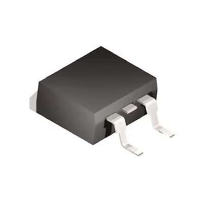
- Use the current onsemi CASE 936 outline and land pattern.
- Treat the large tab as electrically connected to OUTPUT and Pin 2.
- Provide sufficient output-connected copper for worst-case dissipation.
- Keep the programming resistors and bypass components close to the regulator.
The local and production D2PAK JPG files were verified at 20,679 bytes; the production image returned HTTP 200 with image/jpeg content.
Pin Functions
The D2PAK-3 connection follows the onsemi top-view drawing.
The tab is OUTPUT, not ground. Confirm top-view and board-side orientation before layout.
Key Specifications
| Manufacturer | onsemi |
|---|---|
| Function | Adjustable positive linear regulator |
| Output-voltage range | 1.2 V to 37 V |
| Output-current capability | More than 1.5 A; subject to differential voltage and thermal limits |
| Input-output differential limit | 40 V absolute maximum |
| Reference voltage | 1.2 V minimum, 1.25 V typical, 1.3 V maximum |
| Adjustment-pin current | 50 microamperes typical, 100 microamperes maximum |
| Minimum load current | 3.5 mA typical, 10 mA maximum at a 40 V differential |
| Line regulation | 0.01%/V typical and 0.04%/V maximum at 25 degrees C under the stated conditions |
| Load regulation at outputs up to 5 V | 5 mV typical, 25 mV maximum at 25 degrees C under the stated conditions |
| Supply rejection | 65 dB typical without ADJUST bypass; up to 80 dB typical with the stated bypass condition |
| Operating junction temperature | -40 degrees C to 125 degrees C for LM317B |
| Package thermal resistance | 70 degrees C/W junction-to-ambient; 5 degrees C/W junction-to-case for CASE 936 |
| Package and carrier | CASE 936 D2PAK-3, Pb-free, 50 units per rail |
Electrical values apply only under their data-sheet test conditions. Output current is constrained by differential voltage, safe operating area, and thermal dissipation.
Replacement Considerations
Match the adjustable positive-regulator function, ADJUST-OUTPUT-INPUT lead order, output-connected tab, 40 V differential rating, reference tolerance, minimum-load requirement, -40 to 125 degrees C grade, CASE 936 mechanics, and rail packing.
LM317D2TR4G has a different commercial temperature grade, while NCV317BD2TR4G is the automotive-qualified version. TO-220 variants are not footprint substitutes. No internal replacement link is asserted without an exact production-API match.
Manufacturer Information
onsemi documents LM317BD2TG in the LM317/NCV317 family. The exact suffix combination identifies the extended-temperature B grade in Pb-free CASE 936 D2PAK-3 in 50-unit rails.
Applications
Adjustable local rails
Generate board-level voltages using a two-resistor programming network.
Constant-current circuits
Configure the device as a current regulator with an appropriate sense resistor.
Industrial controls
Supply sensors, interfaces, and control electronics across an extended temperature range.
Post regulation
Reduce ripple and set a precise rail after a higher-voltage converter.
Quality & Authenticity
Verify the complete LM317BD2TG code, onsemi marking, CASE 936 geometry, output-connected tab, Pb-free finish, rail label, and date and lot traceability. Distinguish the B, NCV, rail-packed, and TO-220 variants.
FAQ
How is the output voltage set?
Use a resistor from OUTPUT to ADJUST and a second resistor from ADJUST to the load return.
Is the metal tab isolated?
No. The D2PAK tab is electrically connected to OUTPUT.
Can it always deliver 1.5 A?
No. Available current depends on differential voltage, heat spreading, ambient temperature, and protection limits.
What does the B grade mean?
It identifies the extended -40 degrees C to 125 degrees C junction-temperature range.
Are external capacitors useful?
Yes. Input, output, and optional ADJUST bypass capacitors can improve transient and ripple performance; follow the current data-sheet guidance.
Engineering Notice
Before release, validate the resistor network, minimum load, differential voltage, capacitor network, protection-diode need, reverse-discharge paths, tab potential, power dissipation, PCB copper area, junction temperature, rail orientation, and the latest controlled onsemi documentation.
LM317BD2TG Information
- Specifications
- Tags
- Product attributes
- Attribute value
- Manufacturer:
- onsemi
- Series:
- -
- Package/Case:
- TO-263-3, D2PAK (2 Leads + Tab), TO-263AB
- Packaging:
- Tube
- Product Status:
- Active
- Output Configuration:
- Positive
- Output Type:
- Adjustable
- Number of Regulators:
- 1
- Voltage - Input (Max):
- 40V
- Voltage - Output (Min/Fixed):
- 1.2V
- Voltage - Output (Max):
- 37V
- Voltage Dropout (Max):
- -
- Current - Output:
- 1.5A
- Current - Quiescent (Iq):
- 10 mA
- Current - Supply (Max):
- -
- PSRR:
- 80dB ~ 65dB (120Hz)
- Control Features:
- -
- Protection Features:
- Over Current, Over Temperature, Short Circuit
- Operating Temperature:
- -40°C ~ 125°C
- Grade:
- -
- Qualification:
- -
- Mounting Type:
- Surface Mount
- Supplier Device Package:
- D2PAK-3
- Include Parts
- Popular Search
The following parts include "LM317BD2TG" in Silicon Labs LM317BD2TG.
- Part Number
- Manufacturer
- Package
- Description
- MIC5504-1.8YM5-TR Microchip Technology SC-74A, SOT-753 IC REG LINEAR 1.8V 300MA SOT23-5
- MIC5504-3.3YM5-TR Microchip Technology SC-74A, SOT-753 IC REG LINEAR 3.3V 300MA SOT23-5
- MIC5365-3.0YC5-TR Microchip Technology 5-TSSOP, SC-70-5, SOT-353 IC REG LINEAR 3V 150MA SC70-5
- MIC5365-1.8YC5-TR Microchip Technology 5-TSSOP, SC-70-5, SOT-353 IC REG LINEAR 1.8V 150MA SC70-5
- MIC5365-2.5YC5-TR Microchip Technology 5-TSSOP, SC-70-5, SOT-353 IC REG LINEAR 2.5V 150MA SC70-5
- MIC5365-3.3YC5-TR Microchip Technology 5-TSSOP, SC-70-5, SOT-353 IC REG LINEAR 3.3V 150MA SC70-5
- MIC5365-3.3YD5-TR Microchip Technology SOT-23-5 Thin, TSOT-23-5 IC REG LIN 3.3V 150MA TSOT23-5
- MIC5317-3.3YM5-TR Microchip Technology SC-74A, SOT-753 IC REG LINEAR 3.3V 150MA SOT23-5
- TLV1117LV33DCYR Texas Instruments TO-261-4, TO-261AA IC REG LINEAR 3.3V 1A SOT223-4
- MIC5317-3.3YMT-TZ Microchip Technology 4-UDFN Exposed Pad IC REG LINEAR 3.3V 150MA 4DFN
The following parts are popular search parts in Test and Measurement.
Inventory:3,515
Please send an inquiry. Send us your inquiry, and we will respond immediately.


