 Hello! now
 tms@lcdchip.com



QST QE212I

- Part No.:
- QE212I
- Manufacturer:
- QST
- Category:
- Specialized ICs
- Package:
- 8-WFDFN Exposed Pad
- Description:
- 2.0x2.0 EMI SUPPRESSION IC 1.8~3
- Quantity:
Unit Price:$0
Ext Price:$0
- Payment:

- Shipping:


Product Details
QE212I - Active EMI Reduction IC
QST QE212I is an industrial-temperature active EMI-management IC that produces a 1× phase-modulated replica of an input clock. It supports selectable deviation and is supplied in an eight-pin WDFN package, recorded by LCDChip as 8-WFDFN Exposed Pad.
Verify the exact QE212I ordering grade and QST package drawing before design release.
Overview
QE212 uses a non-PLL, phase-controlled active EMI-management architecture to spread the peak energy of an input clock or data source over a controlled band. Its MODOUT pin supplies a 1× phase-modulated output, while SS1 and SS0 select deviation settings. The I suffix in QST's ordering table identifies the industrial grade, specified for -20°C to +85°C.
Key Advantages
Phase modulation reduces narrowband clock energy that contributes to EMI and RFI.
MODOUT retains the input clock's nominal frequency while applying controlled modulation.
SS1 and SS0 let designers tune the trade-off between attenuation and system timing margin.
Pulling PDB low places the device into power-down and makes MODOUT high impedance.
Feature Summary
Non-PLL phase-controlled active EMI management can operate on periodic and aperiodic signals.
QST specifies 20–33 MHz operation at 1.65–2.0 V and 20–55 MHz at 2.5–3.6 V.
Two deviation-select inputs and one active-low power-down input simplify configuration.
Eight-pin WDFN housing supports space-sensitive mobile and embedded platforms.
Package & Footprint
The LCDChip record names 8-WFDFN Exposed Pad. QST's QE212 Rev. 1.03 data sheet specifies an eight-pin WDFN package and provides a WDFN (X208) package-dimension and recommended-footprint drawing. Confirm the manufacturer's dimensions, exposed-pad handling, and pin-1 orientation against the actual board footprint.
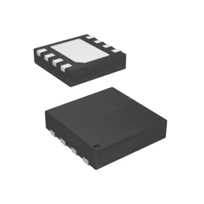
- Match the WDFN X208 land pattern and pin-1 marking.
- Decouple VDD and provide a low-impedance VSS return.
- Control XIN/XOUT and MODOUT routing to preserve clock integrity.
The registered package JPG is unavailable on the production website. Use QST's controlled dimension drawing, not this missing generic image path, for assembly qualification.
Pin Functions
QST's eight-pin QE212 pin-description table assigns:
Crystal oscillator input.
Crystal oscillator output.
Active-low power-down input; low forces MODOUT to high impedance.
System ground reference.
1× phase-modulated buffered output.
Deviation control input with internal pull-up.
Deviation control input with internal pull-down.
System power-supply input.
Configure SS0 and SS1 to a defined logic state using QST's functional table and recommended external connection scheme.
Key Specifications
| Device function | Active clock/data EMI-reduction IC |
|---|---|
| Output | 1× phase-modulated replica at MODOUT |
| Modulation architecture | Non-PLL phase-controlled active EMI management |
| Deviation controls | Two logic inputs: SS1 and SS0 |
| Low-voltage band | 1.65 V to 2.0 V; 20 MHz to 33 MHz |
| Higher-voltage band | 2.5 V to 3.6 V; 20 MHz to 55 MHz |
| Industrial grade | QE212I: -20°C to +85°C per QST ordering information |
| Power-down control | Active-low PDB; MODOUT high impedance when low |
| Typical power-down current | 0.1 µA in the manufacturer's description |
| Package | Eight-pin WDFN; site record 8-WFDFN Exposed Pad |
| Package drawing | QST WDFN (X208), with recommended footprint |
Deviation, jitter, loading, and output performance depend on the operating point and measurement conditions in the QST data sheet.
Replacement Considerations
A replacement must match the input frequency and supply band, output drive and duty cycle, selected deviation behavior, power-down polarity, temperature grade, and exact eight-pin layout. Other QE212 suffixes identify different temperature grades and must not be assumed equivalent for an industrial-temperature design. No unverified LCDChip alternative-product link is asserted here.
Manufacturer Information
QST publishes the QE212 EMI Reduction IC Rev. 1.03 data sheet, including functional configuration, pin description, electrical conditions, QE212I industrial ordering grade, and WDFN package dimensions. Refer to QST's current documentation and notices for controlled specifications.
Applications
Reduce clock-related EMI in power- and space-sensitive handheld designs.
Manage emissions from clock sources in netbooks and mobile internet devices.
Apply a phase-modulated 1× signal when downstream timing margins allow it.
Evaluate selectable deviation alongside shielding, routing, and filtering measures.
Quality & Authenticity
Confirm the QE212I marking, industrial temperature grade, package geometry, lot traceability, and applicable QST documentation. Verify EMI benefit and signal integrity on the assembled product rather than inferring compliance from the component specification alone.
FAQ
Does QE212I change the nominal clock frequency?
It produces a nominal 1× phase-modulated copy of the input; deviation spreads energy around the nominal frequency.
How is deviation selected?
SS1 and SS0 set the deviation mode according to QST's functional table. Validate the resulting timing margins in the full system.
What does PDB do?
Driving PDB low powers down the device and sets MODOUT to a high-impedance state.
What temperature grade is the I suffix?
QST lists QE212I as industrial grade, -20°C to +85°C.
Engineering Notice
Check the VDD/frequency operating band, SS1/SS0 mode, clock-source and output loading, power-down state, WDFN X208 footprint, and system-level EMI results with current QST documentation. The production package JPG returns 404 and must be supplied and visually verified before publication.
QE212I Information
- Specifications
- Tags
- Product attributes
- Attribute value
- Manufacturer:
- QST
- Series:
- QE212
- Package/Case:
- 8-WFDFN Exposed Pad
- Packaging:
- Tape & Reel (TR)
- Product Status:
- Active
- Programmable:
- -
- Type:
- EMI Management IC
- Applications:
- -
- Mounting Type:
- Surface Mount
- Supplier Device Package:
- 8-WDFN (2x2)
- Grade:
- -
- Qualification:
- -
- Include Parts
- Popular Search
The following parts include "QE212I" in Silicon Labs QE212I.
- Part Number
- Manufacturer
- Package
- Description
- CAP200DG-TL Power Integrations 8-SOIC (0.154", 3.90mm Width) IC AUTOMATIC DISCHARGE 8SO
- ATSHA204A-MAHDA-T Microchip Technology 8-UFDFN Exposed Pad IC AUTHENTICATION CHIP 8UDFN
- ATSHA204A-SSHDA-T Microchip Technology 8-SOIC (0.154", 3.90mm Width) IC AUTHENTICATION CHIP 8SOIC
- ATSHA204A-STUCZ-T Microchip Technology TO-236-3, SC-59, SOT-23-3 IC AUTHENTICATION CHIP SOT23-3
- ATECC608B-MAHDA-T Microchip Technology 8-UFDFN Exposed Pad IC AUTHENTICATION CHIP 8UDFN
- ATECC608B-MAHCZ-S Microchip Technology 8-UFDFN Exposed Pad IC AUTHENTICATION CHIP 8UDFN
- ATECC608B-SSHDA-T Microchip Technology 8-SOIC (0.154", 3.90mm Width) IC AUTHENTICATION CHIP 8SOIC
- ATECC608B-MAHDA-S Microchip Technology 8-UFDFN Exposed Pad IC AUTHENTICATION CHIP 8UDFN
- ATECC608A-MAHDA-S Microchip Technology 8-UFDFN Exposed Pad IC AUTHENTICATION CHIP 8UDFN
- ATECC608B-MAVDA-T Microchip Technology 8-UFDFN Exposed Pad IC AUTHENTICATION CHIP 8UDFN
The following parts are popular search parts in Test and Measurement.
Inventory:200
Please send an inquiry. Send us your inquiry, and we will respond immediately.


