 Hello! now
 tms@lcdchip.com



QST QE202I

- Part No.:
- QE202I
- Manufacturer:
- QST
- Category:
- Specialized ICs
- Package:
- 8-WFDFN Exposed Pad
- Description:
- 2.0x2.0 EMI SUPPRESSION IC 1.8~3
- Quantity:
Unit Price:$0
Ext Price:$0
- Payment:

- Shipping:


Product Details
QE202I - Active EMI Reduction IC
QST QE202I is an industrial-temperature, non-PLL active EMI-management IC that produces a nominal 1× phase-modulated clock output. The LCDChip package record is 8-WFDFN Exposed Pad; QST specifies an eight-pin WDFN package.
Verify the QE202I grade and QST WDFN X208 package drawing before design release.
Overview
QE202 uses phase-controlled active EMI management to distribute the peak energy of an input signal over a controlled frequency band. MODOUT provides a nominal 1× phase-modulated output. The QE202I ordering suffix denotes QST's industrial temperature grade of -20°C to +85°C.
Key Advantages
Phase modulation reduces concentrated spectral energy from a clock source.
MODOUT replicates the input's nominal frequency while applying controlled deviation.
SS0 and SS1 provide configuration choices for system-level EMI and timing trade-offs.
Driving PDB low places MODOUT in a high-impedance state.
Feature Summary
Non-PLL, phase-controlled active EMI-management architecture.
QST specifies 10–38 MHz at both 1.65–2.0 V and 2.5–3.6 V supply bands.
Two deviation-select inputs and an active-low power-down input.
Eight-pin WDFN package with QST X208 package drawing.
Package & Footprint
The LCDChip product and package registry name is 8-WFDFN Exposed Pad. QST's QE202 Rev. 1.03 data sheet specifies an eight-pin WDFN package and provides WDFN X208 dimensions and a recommended footprint. Compare the actual pin-1 marking, exposed-pad arrangement and land pattern with QST's drawing.
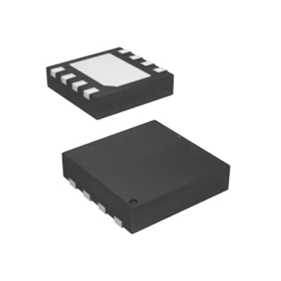
- Use QST's WDFN X208 recommended footprint and pin-1 orientation.
- Decouple VDD locally and provide a low-impedance VSS return.
- Review XIN/XOUT and MODOUT routing for clock integrity.
The registered package JPG is unavailable on the production website; use the controlled QST drawing for footprint qualification.
Pin Functions
QST's QE202 pin-description table assigns:
Crystal oscillator input.
Crystal oscillator output.
Active-low power-down input; low forces MODOUT to high impedance.
System ground reference.
Nominal 1× phase-modulated buffered output.
Deviation control input with internal pull-up.
Deviation control input with internal pull-down.
System power-supply input.
Apply QST's functional table and recommended external connections when defining SS0 and SS1 logic levels.
Key Specifications
| Function | Active clock/data EMI-reduction IC |
|---|---|
| Output | Nominal 1× phase-modulated signal at MODOUT |
| Architecture | Non-PLL phase-controlled active EMI management |
| Deviation selection | SS0 and SS1 logic inputs |
| Low-voltage band | 1.65–2.0 V; 10–38 MHz |
| Higher-voltage band | 2.5–3.6 V; 10–38 MHz |
| Industrial grade | QE202I: -20°C to +85°C per QST ordering table |
| Power-down | Active-low PDB; MODOUT high impedance when low |
| Typical power-save current | 0.1 µA with PDB low, per QST description |
| Package | Eight-pin WDFN; site record 8-WFDFN Exposed Pad |
| Package drawing | QST WDFN X208 |
Use the data-sheet test conditions for deviation, jitter, current and output-drive limits; do not mix typical and maximum values.
Replacement Considerations
A substitute must match supply and frequency band, deviation behavior, power-down polarity, output drive, eight-pin footprint and industrial temperature grade. QE202 suffixes for commercial or automotive grades are not automatically interchangeable. No unverified LCDChip alternative-product link is asserted.
Manufacturer Information
QST's QE202 EMI Reduction IC Rev. 1.03 data sheet documents the pin functions, electrical conditions, QE202I industrial ordering grade and WDFN X208 package drawing. Recheck QST's current controlled documents before qualification.
Applications
Assess clock-related EMI in compact, power-sensitive designs.
Use a nominal 1× modulated clock where downstream timing permits.
Evaluate emissions from clock sources in space-constrained systems.
Compare deviation settings with routing, filtering and shielding options.
Quality & Authenticity
Confirm exact QE202I markings, industrial grade, package geometry and lot traceability against applicable QST documentation. Device-level EMI features do not establish finished-product regulatory compliance.
FAQ
Does QE202I change the nominal clock frequency?
It produces a nominal 1× phase-modulated output; deviation spreads spectral energy around that nominal frequency.
How is deviation configured?
SS0 and SS1 select settings in QST's functional table. Check timing margins in the complete system.
What occurs when PDB is low?
The device enters power-save mode and MODOUT becomes high impedance.
What does the I suffix mean?
QST lists QE202I as industrial grade, -20°C to +85°C.
Engineering Notice
Validate supply/frequency selection, deviation mode, loading, clock routing, power-down behavior, WDFN X208 footprint and system EMI with current QST data. The production package JPG currently returns 404 and must be provided and verified before publication.
QE202I Information
- Specifications
- Tags
- Product attributes
- Attribute value
- Manufacturer:
- QST
- Series:
- QE202
- Package/Case:
- 8-WFDFN Exposed Pad
- Packaging:
- Tape & Reel (TR)
- Product Status:
- Active
- Programmable:
- -
- Type:
- EMI Management IC
- Applications:
- -
- Mounting Type:
- Surface Mount
- Supplier Device Package:
- 8-WDFN (2x2)
- Grade:
- -
- Qualification:
- -
- Include Parts
- Popular Search
The following parts include "QE202I" in Silicon Labs QE202I.
- Part Number
- Manufacturer
- Package
- Description
- CAP200DG-TL Power Integrations 8-SOIC (0.154", 3.90mm Width) IC AUTOMATIC DISCHARGE 8SO
- ATSHA204A-MAHDA-T Microchip Technology 8-UFDFN Exposed Pad IC AUTHENTICATION CHIP 8UDFN
- ATSHA204A-SSHDA-T Microchip Technology 8-SOIC (0.154", 3.90mm Width) IC AUTHENTICATION CHIP 8SOIC
- ATSHA204A-STUCZ-T Microchip Technology TO-236-3, SC-59, SOT-23-3 IC AUTHENTICATION CHIP SOT23-3
- ATECC608B-MAHDA-T Microchip Technology 8-UFDFN Exposed Pad IC AUTHENTICATION CHIP 8UDFN
- ATECC608B-MAHCZ-S Microchip Technology 8-UFDFN Exposed Pad IC AUTHENTICATION CHIP 8UDFN
- ATECC608B-SSHDA-T Microchip Technology 8-SOIC (0.154", 3.90mm Width) IC AUTHENTICATION CHIP 8SOIC
- ATECC608B-MAHDA-S Microchip Technology 8-UFDFN Exposed Pad IC AUTHENTICATION CHIP 8UDFN
- ATECC608A-MAHDA-S Microchip Technology 8-UFDFN Exposed Pad IC AUTHENTICATION CHIP 8UDFN
- ATECC608B-MAVDA-T Microchip Technology 8-UFDFN Exposed Pad IC AUTHENTICATION CHIP 8UDFN
The following parts are popular search parts in Test and Measurement.
Inventory:200
Please send an inquiry. Send us your inquiry, and we will respond immediately.


