 Hello! now
 tms@lcdchip.com



Infineon Technologies PEB2047NV2.1

- Part No.:
- PEB2047NV2.1
- Manufacturer:
- Infineon Technologies
- Category:
- Specialized ICs
- Package:
- 44-LCC (J-Lead)
- Description:
- IC MEMORY 44PLCC
- Quantity:
Unit Price:$0
Ext Price:$0
- Payment:

- Shipping:


Product Details
PEB2047NV2.1 - Memory Time Switch Large
PEB2047NV2.1 is a Siemens-designed, Infineon-listed CMOS memory time switch for PCM telecommunications systems. The manufacturer ordering table identifies the PEB 2047-N V2.1 in a 44-lead P-LCC surface-mount package.
Confirm the full device marking and manufacturer package drawing before replacement or board assembly.
Overview
The PEB 2047 routes PCM input time slots to output time slots using on-chip data and connection memories. At an 8.192 MHz device clock, the data sheet describes switching up to 1024 input channels to 512 output channels. The processor can select constant or minimal channel delay by time slot and access the device through an 8-bit Intel-type or Motorola-type bus.
Key Advantages
PCM switching
Connection memory selects the source for each outgoing time slot.
Delay selection
Constant-frame or minimal delay can be programmed per time slot.
Line alignment
Eight input lines support frame measurement and individually adjustable offsets.
System expansion
Tristate outputs support parallel and tandem switch architectures.
Feature Summary
Serial interfaces
Sixteen PCM input pins and eight PCM output pins are defined in the original pin table.
Processor control
An 8-bit address/data bus supports Intel-type and Motorola-type interface modes.
Diagnostics
A processor-initiated built-in self-test reports through the device status path.
Power
The data sheet specifies a single 5 V supply, with a 5 V plus or minus 5% operating condition.
Package & Footprint
The manufacturer ordering row specifies P-LCC-44 (SMD). LCDChip records the package as 44-LCC (J-Lead), and the local package register maps that name to 44-LCC.jpg. The JPG is currently missing; the image path below is reserved for the verified artwork.
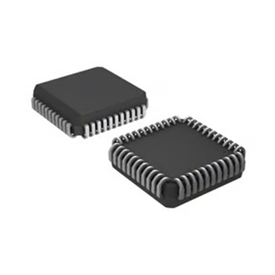
- Use the manufacturer's 44-pin top-view diagram for pin numbering.
- Check the actual J-lead body, land pattern and pin-one marker.
- Do not assume an unrelated 44-pin carrier shares the footprint.
The package JPG and mechanical match must be verified before publication.
Pin Functions
The following groups and pin numbers are taken from the Siemens PEB 2047/2047-16 V2.1 pin table; use its top-view drawing for the full physical layout.
PCM and synchronization
IN0-IN7 use pins 14, 11, 10, 7, 13, 12, 9 and 8. IN8/FS0-IN15/FS7 add eight inputs or frame-measurement functions. SP is pin 3.
PCM outputs
OUT0-OUT7 use pins 38, 37, 43, 42, 36, 35, 41 and 40; the outputs can be tristated.
Processor bus
AD0-AD7 are pins 26, 27 and 29-34; A0/A1 are pins 21/28, CS is pin 22, RD/DS is pin 24, WR/R/W is pin 25, and ALE is pin 2.
Clock, control and power
CLK is pin 44, INT is pin 6, RES is pin 39, VDD is pin 23 and VSS is pin 1.
The shared bus and input pins change function with the selected mode. Verify the configured interface before reusing a board design.
Key Specifications
| Catalog order code | PEB2047NV2.1 |
|---|---|
| Manufacturer ordering row | PEB 2047-N V2.1, Q67100-H6238 |
| Function | Memory Time Switch Large (MTSL) |
| Technology | CMOS |
| Package | P-LCC-44, surface mount |
| Supply condition | 5 V plus or minus 5% |
| Ambient operating range | 0 to 70 degrees C under bias |
| Base-part clock modes | 4.096 or 8.192 MHz; 16.384 MHz functions are -16-only |
| PCM interface | 16 input lines and 8 output lines |
| Switch capacity at 8.192 MHz | Up to 1024 input to 512 output channels |
| Processor interface | 8-bit Intel-type or Motorola-type |
| Output mode | Tristate-capable PCM outputs |
Capacity and timing depend on clock and mode. Consult the original tables when designing a new configuration.
Replacement Considerations
The PEB 2047-16 belongs to the same documented family but adds 16.384 MHz functions; it is not an unconditional substitute. Verify the full ordering code, interface mode, supply and timing, package drawing, temperature grade and firmware register programming before substitution. No unverified internal alternative link is included.
Manufacturer Information
The 03.95 edition of the Siemens Semiconductor Group PEB 2047/PEB 2047-16 Version 2.1 data sheet contains the PEB 2047-N V2.1 ordering row, feature list, pin table and electrical conditions used here. Infineon is the catalog manufacturer for this legacy Siemens device. Confirm the version and marking on the actual supplied lot.
Applications
PCM exchanges
Time-slot routing in legacy digital telecommunications switches.
Voice-channel switching
Programmable minimal-delay routing for PCM voice paths.
Frame-aligned systems
Input-offset measurement and adjustment for differing line delays.
Installed-equipment support
Qualified maintenance of systems already designed for the PEB 2047-N.
Quality & Authenticity
Inspect the complete device marking, revision, date/lot code and 44-lead J-lead condition. Verify traceability and storage handling for legacy inventory. This listing does not assert new production, electrical retest or an undisclosed certification.
FAQ
Does this base model support 16.384 MHz?
No. The manufacturer reserves the 16.384 MHz functions for the PEB 2047-16.
How many PCM lines are provided?
The pin table identifies 16 input lines and eight tristate-capable output lines.
Which processor bus is supported?
The 8-bit bus supports Intel-type and Motorola-type modes with different control-pin functions.
Is the package image ready?
No. The registered 44-LCC.jpg is absent locally and must be supplied and checked.
Engineering Notice
Keep this detail under review until the registered package JPG, physical footprint, supplied-lot marking and current distributor quote are verified. Do not publish while the package image or pricing checks remain open.
PEB2047NV2.1 Information
- Specifications
- Tags
- Product attributes
- Attribute value
- Manufacturer:
- Infineon Technologies
- Series:
- -
- Package/Case:
- 44-LCC (J-Lead)
- Packaging:
- Bulk
- Product Status:
- Active
- Programmable:
- Not Verified
- Type:
- Memory
- Applications:
- -
- Mounting Type:
- Surface Mount
- Supplier Device Package:
- 44-PLCC (16.6x16.6)
- Grade:
- -
- Qualification:
- -
- Include Parts
- Popular Search
The following parts include "PEB2047NV2.1" in Silicon Labs PEB2047NV2.1.
- Part Number
- Manufacturer
- Package
- Description
- CAP200DG-TL Power Integrations 8-SOIC (0.154", 3.90mm Width) IC AUTOMATIC DISCHARGE 8SO
- ATSHA204A-MAHDA-T Microchip Technology 8-UFDFN Exposed Pad IC AUTHENTICATION CHIP 8UDFN
- ATSHA204A-SSHDA-T Microchip Technology 8-SOIC (0.154", 3.90mm Width) IC AUTHENTICATION CHIP 8SOIC
- ATSHA204A-STUCZ-T Microchip Technology TO-236-3, SC-59, SOT-23-3 IC AUTHENTICATION CHIP SOT23-3
- ATECC608B-MAHDA-T Microchip Technology 8-UFDFN Exposed Pad IC AUTHENTICATION CHIP 8UDFN
- ATECC608B-MAHCZ-S Microchip Technology 8-UFDFN Exposed Pad IC AUTHENTICATION CHIP 8UDFN
- ATECC608B-SSHDA-T Microchip Technology 8-SOIC (0.154", 3.90mm Width) IC AUTHENTICATION CHIP 8SOIC
- ATECC608B-MAHDA-S Microchip Technology 8-UFDFN Exposed Pad IC AUTHENTICATION CHIP 8UDFN
- ATECC608A-MAHDA-S Microchip Technology 8-UFDFN Exposed Pad IC AUTHENTICATION CHIP 8UDFN
- ATECC608B-MAVDA-T Microchip Technology 8-UFDFN Exposed Pad IC AUTHENTICATION CHIP 8UDFN
The following parts are popular search parts in Test and Measurement.
Inventory:106
Please send an inquiry. Send us your inquiry, and we will respond immediately.


