 Hello! now
 tms@lcdchip.com



NXP USA Inc. MCZ33905CS3EK
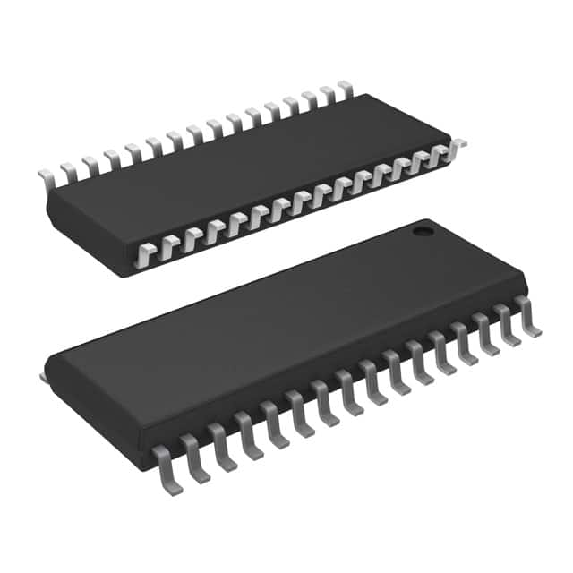
- Part No.:
- MCZ33905CS3EK
- Manufacturer:
- NXP USA Inc.
- Category:
- Specialized ICs
- Package:
- 32-SSOP (0.295", 7.50mm Width) Exposed Pad
- Description:
- IC INTERFACE SPECIALIZED 32SOIC
- Quantity:
Unit Price:$0
Ext Price:$0
- Payment:

- Shipping:


Product Details
MCZ33905CS3EK - 3.3 V CAN and LIN System Basis Chip
MCZ33905CS3EK is an NXP 33905S-family system basis chip for automotive microcontroller power management, high-speed CAN and one LIN interface. The exact legacy order code uses a 32-pin exposed-pad SOIC-class package, recorded in the LCDChip catalog as 32-SSOP Exposed Pad.
NXP's current family data sheet lists the newer D-version order code and records removal of the C-version from the current orderable table. Verify the legacy C-version lifecycle and package drawing for the exact stock being purchased.
Overview
The 33905S combines a microcontroller supply regulator, high-speed CAN transceiver, single LIN transceiver, watchdog, wake-up resources and fail-safe functions in one automotive system basis chip. The CS3EK code denotes the C-version, 3.3 V VDD option and 32-pin exposed package. It is intended to consolidate essential power and communication functions around a vehicle control microcontroller.
Key Advantages
Combines high-speed CAN with one LIN interface in the 33905S configuration.
Provides the 3.3 V VDD version for a compatible microcontroller power rail.
The family supports controlled reduced-power operation and wake-up monitoring.
Watchdog, reset, interrupt and SAFE-related functions support a validated system safety concept.
Feature Summary
The S variant includes one LIN interface; it is not the dual-LIN 33905D version.
Manufacturer ordering information describes three wake-up inputs with one LIN master termination, or four wake-up inputs without that termination.
SPI signals configure device operation and report diagnostic status to the host MCU.
The 32-pin SOIC-class exposed package provides the grounding and thermal interface defined by the NXP footprint.
Package & Footprint
LCDChip's original record describes 32-SSOP (0.295 inch, 7.50 mm width) Exposed Pad, normalized by the package workbook to 32-SSOP Exposed Pad. DigiKey identifies the supplier package as 32-SOIC-EP, while NXP identifies the 33905S package as a 32-pin exposed SOIC, SOT1746-3 in its current family table. These naming layers require a drawing-level footprint check for the exact legacy CS3EK device.

- Confirm the NXP drawing and land pattern for the exact device.
- Check exposed-pad grounding and thermal layout.
- Verify pin-one orientation and the difference between catalog case and supplier package names.
The registered JPG is currently missing locally. Add and inspect the image before publication.
Pin Functions
The named signals below follow NXP's 33905S 32-pin connection diagram and family pin-definition table. Use the manufacturer's numbered top-view drawing for PCB placement.
Battery-related supply inputs, regulated MCU supply output and package/lead-frame return connections.
High-speed CAN bus pair and microcontroller transmit/receive logic signals.
Single LIN bus connection, host logic interface and configurable LIN termination/wake input.
SPI command/data interface used to configure and diagnose the system basis chip.
Reset, interrupt, fail-safe and debug-related system-control signals.
Sense, multiplexed monitoring and configurable wake/general-purpose connections as defined in the NXP pin table.
Some pin functions are multiplexed or mode-dependent. Confirm register configuration and the exact numbered pin assignment before wiring.
Key Specifications
| Device family | NXP 33905S system basis chip, legacy C-version |
|---|---|
| MCU supply option | 3.3 V VDD option in the CS3EK order code |
| CAN interface | One integrated high-speed CAN transceiver |
| LIN interfaces | One integrated LIN interface in the S configuration |
| Wake/termination options | Three wake inputs plus one LIN master termination, or four wake inputs without LIN termination, per family ordering table |
| Control interface | SPI with MOSI, MISO, SCLK and CS signals |
| Operating ambient rating | -40 to +125 degrees C, NXP MC33905 orderable-family table |
| LIN supply range | 7.0 to 18 V VSUP, LIN characteristics conditions; not the absolute maximum |
| LIN VBAT operating range | 8.0 to 18 V in the documented LIN characteristics table |
| Package | 32-pin exposed-pad SOIC-class; verify exact CS3EK drawing against catalog 32-SSOP Exposed Pad name |
| Lifecycle | C-version removed from current NXP orderable table; distributor lists exact part obsolete |
The LIN electrical-characteristics conditions are not a universal operating-voltage specification for every integrated block. Apply the full data-sheet limits, thermal derating and external-component rules to the final design.
Replacement Considerations
NXP's current family table recommends the 33905 D-version for new designs and states that the C and D versions have no electrical-parameter specification changes, but the D version includes quality improvements. MCZ33905DS3EK exists in the LCDChip catalog as a distinct unpublished product. It still requires confirmation of order-code packaging, qualification, software behavior and customer approval; no automatic drop-in claim is made.
MCZ33905CS5EK and MCZ33904C3EK also exist as distinct unpublished LCDChip models. The former has a 5.0 V rather than 3.3 V VDD option; the latter belongs to a different family configuration. Neither is a direct replacement without MCU rail, CAN/LIN, wake-input, pinout and safety analysis. No internal links are inserted to these unpublished entries.
Manufacturer Information
NXP Semiconductors maintains the MC33903/MC33904/MC33905 family data sheet and an exact MCZ33905CS3EK product record. The current data-sheet revision removes legacy C-version order codes from its ordering table and directs new designs toward the D revision. Procurement of this obsolete exact model should include date-code, authenticity and lifecycle checks.
Applications
Provide MCU power and network interfaces in a qualified vehicle control module.
Combine communication, wake-up monitoring and diagnostics around a host controller.
Use documented low-power modes and wake events in a validated battery budget.
Source exact C-version stock for an already qualified design while checking traceability.
Quality & Authenticity
Verify the complete MCZ33905CS3EK marking, exposed-pad package, tube packaging, date code and manufacturer traceability. Obsolete or last-stock devices need heightened authenticity review. Match the actual package and electrical revision to the previously approved ECU bill of materials; an illustrative JPG is not sufficient proof.
FAQ
How many LIN channels does this part provide?
The 33905S configuration provides one LIN interface alongside high-speed CAN.
Is its MCU rail 3.3 V or 5 V?
The CS3EK order code denotes the 3.3 V VDD option. Verify the host MCU's full power requirements against the data sheet.
Can MCZ33905DS3EK be substituted automatically?
No. NXP recommends the D version for new designs, but the complete design, qualification and purchase order must be reviewed.
Is the catalog package image available?
No. The registered 32-SSOP Exposed Pad JPG is missing and its footprint mapping requires visual verification.
Engineering Notice
Use NXP's current family data sheet, package drawing, errata and product-change notices for engineering sign-off. Check the legacy C-version against the D-version before any redesign. Distributor stock and tier prices must be confirmed from a fresh exact-part quote before synchronization; the registered package JPG is missing, so this product must remain unpublished pending review.
MCZ33905CS3EK Information
- Specifications
- Tags
- Product attributes
- Attribute value
- Manufacturer:
- NXP USA Inc.
- Series:
- -
- Package/Case:
- 32-SSOP (0.295", 7.50mm Width) Exposed Pad
- Packaging:
- Tube
- Product Status:
- Obsolete
- Programmable:
- -
- Type:
- -
- Applications:
- System Basis Chip
- Mounting Type:
- Surface Mount
- Supplier Device Package:
- 32-SOIC-EP
- Grade:
- -
- Qualification:
- -
- Include Parts
- Popular Search
The following parts include "MCZ33905CS3EK" in Silicon Labs MCZ33905CS3EK.
- Part Number
- Manufacturer
- Package
- Description
- CAP200DG-TL Power Integrations 8-SOIC (0.154", 3.90mm Width) IC AUTOMATIC DISCHARGE 8SO
- ATSHA204A-MAHDA-T Microchip Technology 8-UFDFN Exposed Pad IC AUTHENTICATION CHIP 8UDFN
- ATSHA204A-SSHDA-T Microchip Technology 8-SOIC (0.154", 3.90mm Width) IC AUTHENTICATION CHIP 8SOIC
- ATSHA204A-STUCZ-T Microchip Technology TO-236-3, SC-59, SOT-23-3 IC AUTHENTICATION CHIP SOT23-3
- ATECC608B-MAHDA-T Microchip Technology 8-UFDFN Exposed Pad IC AUTHENTICATION CHIP 8UDFN
- ATECC608B-MAHCZ-S Microchip Technology 8-UFDFN Exposed Pad IC AUTHENTICATION CHIP 8UDFN
- ATECC608B-SSHDA-T Microchip Technology 8-SOIC (0.154", 3.90mm Width) IC AUTHENTICATION CHIP 8SOIC
- ATECC608B-MAHDA-S Microchip Technology 8-UFDFN Exposed Pad IC AUTHENTICATION CHIP 8UDFN
- ATECC608A-MAHDA-S Microchip Technology 8-UFDFN Exposed Pad IC AUTHENTICATION CHIP 8UDFN
- ATECC608B-MAVDA-T Microchip Technology 8-UFDFN Exposed Pad IC AUTHENTICATION CHIP 8UDFN
The following parts are popular search parts in Test and Measurement.
Inventory:175
Please send an inquiry. Send us your inquiry, and we will respond immediately.


