 Hello! now
 tms@lcdchip.com



NXP Semiconductors MCZ33903DP3EK
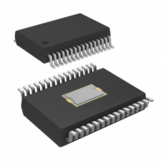
- Part No.:
- MCZ33903DP3EK
- Manufacturer:
- NXP Semiconductors
- Category:
- Specialized ICs
- Package:
- 32-SSOP (0.295", 7.50mm Width) Exposed Pad
- Description:
- MCZ33903DP3EK - System Basis Chi
- Quantity:
Unit Price:$0
Ext Price:$0
- Payment:

- Shipping:


Product Details
MCZ33903DP3EK - 3.3 V CAN System Basis Chip
NXP Semiconductors MCZ33903DP3EK integrates a high-speed CAN interface, MCU supply regulation, wake-up management, and SPI-controlled system functions in a 32-SSOP exposed-pad package.
The exact order code and package designation were checked against NXP-controlled product and package information. Verify the final design against the current NXP datasheet and ordering documentation.
Overview
MCZ33903DP3EK is the 3.3 V MC33903P variant in NXP's second-generation system basis chip family. It combines the functions commonly needed around an automotive microcontroller: battery-supplied power management, an enhanced high-speed CAN physical interface, wake-up inputs, reset and interrupt signaling, and a serial configuration interface. NXP's orderable-part table identifies the P version as a no-LIN configuration with three wake-up inputs; do not assume features of the S or D LIN variants are present.
Key Advantages
Combines MCU supply, high-speed CAN transceiver, monitoring, and system control functions.
The DP3EK orderable variant is specified with a 3.3 V VDD output.
The P variant offers three wake-up inputs for system-state control.
SPI access lets the host configure and monitor system basis functions.
Feature Summary
Integrated enhanced high-speed CAN bus interface with CANH, CANL, TXD, and RXD connections.
Battery-supply input, regulated VDD output, reset, and fail-safe support for the host system.
Interrupt and diagnostic functions are controlled and observed through the MCU interface.
MC33903P is a no-LIN variant; LIN functions shown for other family members must not be copied into this design.
Package & Footprint
The catalog package is 32-SSOP Exposed Pad. NXP identifies the exact part with package version SOT1762-2 (SSOP32). The package drawing describes a 32-terminal, 0.65 mm-pitch body approximately 11 mm by 7.5 mm by 2.3 mm. Use the controlled drawing and recommended land pattern for board layout; the exposed ground lead frame needs the specified thermal and electrical connection.

- Match SOT1762-2 terminal numbering and exposed-pad geometry.
- Check pad soldering and ground-return recommendations in the NXP package drawing.
- Keep CAN bus routing, protection, and termination consistent with the system schematic.
Package image pending: the registered JPG is absent locally and the production image URL currently returns HTTP 404. This draft must not be published until the actual image is available and verified.
Pin Functions
The following groups summarize functions shown for the MC33903P in the NXP pin-connection and pin-definition sections. Use the NXP pin-number table, not this summary, when assigning schematic nets.
Battery-related supply input and regulated MCU supply output.
High-speed CAN bus pair and MCU transmit/receive interface.
Four-wire SPI chip select, clock, data input, and data output.
Host reset, interrupt, and safety-related signaling.
Configurable input/output and wake-up resources of the P variant.
Ground references and exposed package connection.
The exact pin numbers, no-connect treatment, and operating-mode functions must be verified from the MC33903P drawing and Table 4 of the current datasheet.
Key Specifications
| Orderable model | MCZ33903DP3EK |
|---|---|
| Manufacturer | NXP Semiconductors |
| Device family | MC33903 second-generation system basis chip |
| Variant | MC33903P, no LIN interface |
| VDD output option | 3.3 V nominal orderable variant |
| CAN function | Enhanced high-speed CAN physical interface |
| Wake-up input option | Three wake-up inputs for the P variant |
| Host configuration | SPI |
| Ambient rating in orderable table | -40 °C to +125 °C |
| Package version | SOT1762-2 / 32-SSOP exposed-pad catalog designation |
| Package terminal pitch | 0.65 mm per NXP package drawing |
Electrical thresholds, regulator load limits, CAN timing, and typical currents vary by operating mode and test conditions; consult the applicable NXP electrical-characteristics tables before component selection.
Replacement Considerations
NXP lists other MC33903 orderable variants, but they are not unconditional replacements. A 5.0 V VDD variant changes the MCU supply, while S and D variants add LIN functions and can change pin usage and system behavior. Compare the complete suffix, package version, exposed-pad footprint, power rails, CAN behavior, SPI configuration, temperature range, and required safety behavior before any substitution. No internal catalog replacement link is asserted here because an exact candidate catalog match and compatibility assessment have not been completed.
Manufacturer Information
NXP Semiconductors documents MCZ33903DP3EK in its MC33903/MC33904/MC33905 family documentation and exact-part product-content declaration. Refer to the current controlled datasheet, package drawing, and any applicable product-change notices when qualifying this order code.
Applications
MCU-based modules needing power supervision and a high-speed CAN physical connection.
Distributed control nodes with wake-up inputs and low-power state control.
Systems that can meet the device's electrical, EMC, and qualification requirements.
Quality & Authenticity
Confirm the complete NXP order code, top marking, package version, and traceability documents during incoming inspection. A catalog listing alone does not establish automotive qualification, application fitness, or authorized-channel provenance. Check the current manufacturer documentation and project-specific quality requirements before approval.
FAQ
Does MCZ33903DP3EK include LIN?
No. NXP's MC33903P orderable-part table specifies zero LIN interfaces for this variant.
What MCU rail is associated with DP3EK?
The orderable-part table identifies a 3.3 V VDD output option. Confirm load and voltage limits in the electrical tables for the intended operating mode.
Can another MC33903 suffix be substituted automatically?
No. Check supply voltage, LIN content, pin use, package, control settings, and qualification for the complete order code.
Is the package image verified?
No. The production package JPG is currently unavailable, so publication is blocked pending image verification.
Engineering Notice
Use this page as a selection summary, not as a substitute for the latest NXP datasheet, package drawing, or application validation. Confirm the full order code, actual silicon revision, electrical limits, thermal path, EMC behavior, and CAN system design. The missing production package image prevents publication of this draft.
MCZ33903DP3EK Information
- Specifications
- Tags
- Product attributes
- Attribute value
- Manufacturer:
- NXP Semiconductors
- Series:
- -
- Package/Case:
- 32-SSOP (0.295", 7.50mm Width) Exposed Pad
- Packaging:
- Bulk
- Product Status:
- Active
- Programmable:
- -
- Type:
- -
- Applications:
- System Basis Chip
- Mounting Type:
- Surface Mount
- Supplier Device Package:
- 32-SOIC-EP
- Grade:
- Automotive
- Qualification:
- -
- Include Parts
- Popular Search
The following parts include "MCZ33903DP3EK" in Silicon Labs MCZ33903DP3EK.
- Part Number
- Manufacturer
- Package
- Description
- CAP200DG-TL Power Integrations 8-SOIC (0.154", 3.90mm Width) IC AUTOMATIC DISCHARGE 8SO
- ATSHA204A-MAHDA-T Microchip Technology 8-UFDFN Exposed Pad IC AUTHENTICATION CHIP 8UDFN
- ATSHA204A-SSHDA-T Microchip Technology 8-SOIC (0.154", 3.90mm Width) IC AUTHENTICATION CHIP 8SOIC
- ATSHA204A-STUCZ-T Microchip Technology TO-236-3, SC-59, SOT-23-3 IC AUTHENTICATION CHIP SOT23-3
- ATECC608B-MAHDA-T Microchip Technology 8-UFDFN Exposed Pad IC AUTHENTICATION CHIP 8UDFN
- ATECC608B-MAHCZ-S Microchip Technology 8-UFDFN Exposed Pad IC AUTHENTICATION CHIP 8UDFN
- ATECC608B-SSHDA-T Microchip Technology 8-SOIC (0.154", 3.90mm Width) IC AUTHENTICATION CHIP 8SOIC
- ATECC608B-MAHDA-S Microchip Technology 8-UFDFN Exposed Pad IC AUTHENTICATION CHIP 8UDFN
- ATECC608A-MAHDA-S Microchip Technology 8-UFDFN Exposed Pad IC AUTHENTICATION CHIP 8UDFN
- ATECC608B-MAVDA-T Microchip Technology 8-UFDFN Exposed Pad IC AUTHENTICATION CHIP 8UDFN
The following parts are popular search parts in Test and Measurement.
Inventory:1,260
Please send an inquiry. Send us your inquiry, and we will respond immediately.


