 Hello! now
 tms@lcdchip.com



Analog Devices Inc./Maxim Integrated MAX5426CEUD+

- Part No.:
- MAX5426CEUD+
- Manufacturer:
- Analog Devices Inc./Maxim Integrated
- Category:
- Specialized ICs
- Package:
- 14-TSSOP (0.173", 4.40mm Width)
- Description:
- IC RESISTOR NETWORK 14TSSOP
- Quantity:
Unit Price:$0
Ext Price:$0
- Payment:

- Shipping:


Product Details
MAX5426CEUD+ - Precision Resistor Network for Programmable Instrumentation Amplifiers
The Analog Devices / Maxim Integrated MAX5426CEUD+ is a C-grade, digitally selectable precision resistor network for a three-op-amp instrumentation-amplifier circuit. It provides gain settings of 1, 2, 4 and 8 in a 14-pin TSSOP.
The exact orderable model is listed on the manufacturer's MAX5426 product page; functional and electrical details follow the manufacturer's MAX5426 Rev. 0 data sheet. Check the manufacturer's current lifecycle notice before selecting it for a new design.
Overview
MAX5426CEUD+ integrates precision fixed and digitally controlled resistors used around external amplifiers. Two logic inputs select the network's differential gain. The part is a resistor network, not a complete instrumentation amplifier; the external op amps, feedback connections, supply rails and common-mode range determine the complete circuit's behavior.
Key Advantages
Four selected gains
D1 and D0 choose differential gains of 1, 2, 4 or 8 without replacing the external resistor network.
C-grade accuracy
The manufacturer's C-grade gain-range accuracy limit is 0.5% under the stated test setup.
Simple logic control
A two-bit CMOS/TTL-compatible parallel interface controls gain selection.
Compact integration
A 14-pin TSSOP combines the precision network and control elements for space-conscious amplifier layouts.
Feature Summary
Gain truth table
D1:D0 = 00, 01, 10 and 11 select gains of 1, 2, 4 and 8, respectively.
Supply arrangement
Designed for dual supply operation from approximately ±5 V to ±15 V; observe the detailed VDD and VSS limits.
Offset and common mode
OFFSET permits an applied DC offset; CM is the common-mode reference connection in the illustrated amplifier topology.
External signal chain
The network connects to external input buffers and a differential output amplifier rather than driving a load on its own.
Package & Footprint
The manufacturer lists MAX5426CEUD+ in a 14-pin TSSOP. The LCDChip package registry normalizes the database description to 14-TSSOP; confirm body, lead pitch and land pattern against the manufacturer package drawing before PCB release.
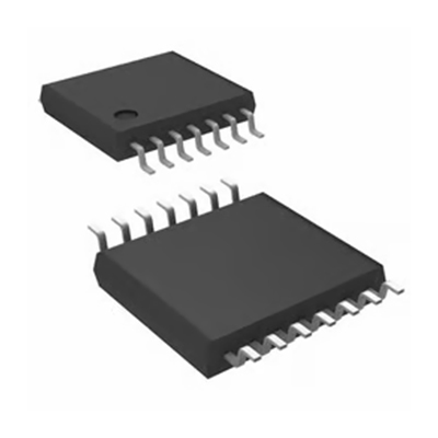
- Confirm pin 1 orientation and the manufacturer's 14-pin pinout.
- Place the specified 0.1 µF supply bypass capacitors close to VDD and VSS.
- Route precision analog nodes away from switching logic where practical.
The registered package image is not yet present in the local JPG library; verify the image after it is supplied.
Pin Functions
The manufacturer's 14-pin top-view pin description identifies these connections:
1 VDD; 2 GND; 3 VSS
Positive supply, ground and negative supply. Bypass each supply to ground as specified.
4 FB2; 5 OUT2
Positive-side first-stage feedback/input and output network connections.
6 OFFSET; 7 INDIF-; 8 INDIF+
Output-stage offset input and negative/positive differential-amplifier input connections.
9 OUT; 10 OUT1; 11 FB1
Final output-network terminal and negative-side first-stage output/feedback connections.
12 CM; 13 D0; 14 D1
Common-mode node and two digital gain-select inputs.
Use the data-sheet pin drawing and recommended application circuit for the exact board wiring; network pin names do not replace a full external-amplifier schematic.
Key Specifications
| Device class | Precision resistor network for programmable instrumentation amplifiers |
|---|---|
| Orderable grade | MAX5426C, 0.5% maximum gain-range accuracy under data-sheet test conditions |
| Differential gain selections | 1, 2, 4, 8 |
| Digital gain control | Two-bit parallel, D1 and D0 |
| Positive supply range | VDD = 4.75 V to 15.75 V relative to ground |
| Negative supply range | VSS = -15.75 V to -4.75 V relative to ground |
| Positive supply current | 36 µA typical, 80 µA maximum with D1 = D0 = 5 V at specified conditions |
| Digital input high | 2.4 V minimum at specified conditions |
| Digital input low | 0.8 V maximum at specified conditions |
| Switching time | 60 ns typical under the data-sheet timing definition |
| Operating temperature | -40 °C to +85 °C |
| Package | 14-pin TSSOP |
Electrical table conditions are VDD = +15 V, VSS = -15 V, GND = 0 V and TA across the stated operating range unless noted; typical values are at +25 °C. Absolute-maximum ratings are stress limits, not recommended operating conditions.
Replacement Considerations
The manufacturer's MAX5426A and MAX5426B grades share the family function and 14-pin TSSOP option, but their gain-accuracy specifications differ from this C-grade orderable model. A grade change is not an automatic substitute: confirm complete ordering code, package, lifecycle, gain error allocation, logic thresholds, supplies and production qualification. No unverified LCDChip internal replacement link is provided.
Manufacturer Information
MAX5426 originated with Maxim Integrated and is documented by Analog Devices. The manufacturer's orderable-model listing includes MAX5426CEUD+. Refer to the current Analog Devices product page for lifecycle and controlled documents, and to the Rev. 0 data sheet for the circuit, pinout and limits.
Applications
Programmable instrumentation amplifiers
Selectable gain in an externally implemented three-op-amp measurement front end.
RF amplifier gain control
Precision resistor selection in suitable RF power-amplifier control circuits.
Precision dual attenuation
Matched-network use where the manufacturer's application circuit and error budget fit.
Measurement channel configuration
Digital selection of analog gain across operating modes without mechanical resistor changes.
Quality & Authenticity
Verify the complete marking, package geometry and traceability against the manufacturer-controlled documentation and purchase records. Treat handling, soldering and acceptance as separate checks. This page does not establish qualification or authenticity of an individual unit.
FAQ
Is MAX5426CEUD+ a complete instrumentation amplifier?
No. It is a precision resistor network that works with external operational amplifiers in the manufacturer's application topology.
How is gain selected?
Logic inputs D1 and D0 select gains 1, 2, 4 or 8 according to the data-sheet truth table.
What distinguishes the C grade?
The C-grade gain-range accuracy limit is 0.5% under the manufacturer's specified test conditions; A and B grades have different limits.
Can a related MAX5426 grade be fitted without review?
No. Check the full ordering code and system-level gain, supply, package and lifecycle requirements before substitution.
Engineering Notice
Validate the current manufacturer data sheet, lifecycle status, exact package drawing, external amplifier choices, digital-input levels and thermal limits for the final design. The package JPG referenced here requires verification when supplied.
MAX5426CEUD+ Information
- Specifications
- Tags
- Product attributes
- Attribute value
- Manufacturer:
- Analog Devices Inc./Maxim Integrated
- Series:
- -
- Package/Case:
- 14-TSSOP (0.173", 4.40mm Width)
- Packaging:
- Tube
- Product Status:
- Last Time Buy
- Programmable:
- Not Verified
- Type:
- Resistor Network
- Applications:
- Instrumentation Amplifiers
- Mounting Type:
- Surface Mount
- Supplier Device Package:
- 14-TSSOP
- Grade:
- -
- Qualification:
- -
- Include Parts
- Popular Search
The following parts include "MAX5426CEUD+" in Silicon Labs MAX5426CEUD+.
- Part Number
- Manufacturer
- Package
- Description
- CAP200DG-TL Power Integrations 8-SOIC (0.154", 3.90mm Width) IC AUTOMATIC DISCHARGE 8SO
- ATSHA204A-MAHDA-T Microchip Technology 8-UFDFN Exposed Pad IC AUTHENTICATION CHIP 8UDFN
- ATSHA204A-SSHDA-T Microchip Technology 8-SOIC (0.154", 3.90mm Width) IC AUTHENTICATION CHIP 8SOIC
- ATSHA204A-STUCZ-T Microchip Technology TO-236-3, SC-59, SOT-23-3 IC AUTHENTICATION CHIP SOT23-3
- ATECC608B-MAHDA-T Microchip Technology 8-UFDFN Exposed Pad IC AUTHENTICATION CHIP 8UDFN
- ATECC608B-MAHCZ-S Microchip Technology 8-UFDFN Exposed Pad IC AUTHENTICATION CHIP 8UDFN
- ATECC608B-SSHDA-T Microchip Technology 8-SOIC (0.154", 3.90mm Width) IC AUTHENTICATION CHIP 8SOIC
- ATECC608B-MAHDA-S Microchip Technology 8-UFDFN Exposed Pad IC AUTHENTICATION CHIP 8UDFN
- ATECC608A-MAHDA-S Microchip Technology 8-UFDFN Exposed Pad IC AUTHENTICATION CHIP 8UDFN
- ATECC608B-MAVDA-T Microchip Technology 8-UFDFN Exposed Pad IC AUTHENTICATION CHIP 8UDFN
The following parts are popular search parts in Test and Measurement.
Inventory:2,232
Please send an inquiry. Send us your inquiry, and we will respond immediately.


