 Hello! now
 tms@lcdchip.com



Analog Devices Inc./Maxim Integrated MAX25400GTC/V+
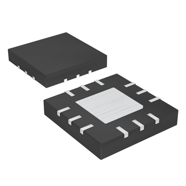
- Part No.:
- MAX25400GTC/V+
- Manufacturer:
- Analog Devices Inc./Maxim Integrated
- Category:
- Specialized ICs
- Package:
- 12-WFQFN Exposed Pad
- Description:
- IC USB PORT PROTECTOR 12TQFN
- Quantity:
Unit Price:$0
Ext Price:$0
- Payment:

- Shipping:


Product Details
MAX25400GTC/V+ - Automotive Hi-Speed USB 2.0 Protector
MAX25400GTC/V+ from Analog Devices / Maxim Integrated protects automotive USB 2.0 D+ and D- lines against connector-side overvoltage and electrostatic discharge. The exact ordering code specifies a 12-pin, 3 mm × 3 mm TQFN exposed-pad package; the LCDChip catalog describes it as 12-WFQFN Exposed Pad.
Technical characteristics below are based on the manufacturer's MAX25400 Rev. 1 data sheet and exact ordering table. Confirm the land pattern against the controlled package drawing before PCB release.
Overview
The MAX25400 places two low-resistance USB 2.0 data switches between a low-voltage transceiver and the external connector. It supports high-speed, full-speed, and low-speed signaling while monitoring the protected HVD+ and HVD- pins for overvoltage. A detected data-line fault, BUS undervoltage, or overtemperature condition disables the switches and asserts the open-drain FAULT output.
Key Advantages
Connector-side HVD+ and HVD- tolerate short-to-BUS and short-to-battery events within the manufacturer's stated limits.
Supports 480 Mbps high-speed, 12 Mbps full-speed, and 1.5 Mbps low-speed operation.
Open-drain FAULT indicates protected-line overvoltage, BUS undervoltage, or thermal shutdown.
Exact part uses a 12-pin, 3 mm × 3 mm exposed-pad TQFN package rated for -40°C to +105°C ambient operation.
Feature Summary
Two 3.3 Ω typical on-resistance data switches connect D+/D- to HVD+/HVD- when no fault is present.
Protected connector pins are characterized to ±25 kV IEC 61000-4-2 air-gap and ±8 kV contact discharge.
BUS undervoltage lockout has a 4.2 V typical falling threshold; the data switches become high impedance below the threshold.
The manufacturer identifies this family as AEC-Q100 qualified; verify the exact procurement and qualification documents for the intended program.
Package & Footprint
LCDChip's original catalog package is 12-WFQFN Exposed Pad; the package register uses the same canonical name. The manufacturer's ordering table calls MAX25400GTC/V+ a 12-pin TQFN-EP, 3 mm × 3 mm. The two naming systems should not be assumed mechanically interchangeable without checking the manufacturer's package drawing, pad geometry, exposed-pad connection, and assembly requirements.

- Confirm the 12-pin TQFN-EP controlled land pattern, orientation, and exposed-pad grounding.
- Keep the protected HVD pair close to the connector and route the USB differential pair as controlled-impedance, length-matched traces.
- Place BUS and IN bypass capacitors close to their pins and ground return.
The referenced package JPG is currently missing from both the local image directory and the production site; verify and add the correct image before publication.
Pin Functions
Pin assignments follow the MAX25400 Rev. 1 data-sheet pin description for the 12-pin TQFN package.
High-voltage-protected connector-side USB D+ and D- outputs.
Open-drain fault indicator; use an external pull-up to IN as shown by the manufacturer.
BUS is the USB 5 V supply; IN is the 3.0 V to 3.6 V logic supply.
Low-voltage transceiver-side differential data connections.
Ground connections; also review exposed-pad requirements in the package drawing.
No external connection; internally connected to IC ground according to the data sheet.
Verify pin-1 orientation, ground network, and the exact package drawing during schematic and PCB review.
Key Specifications
| Function | Automotive USB 2.0 data-line protector |
|---|---|
| Exact package | 12-pin, 3 mm × 3 mm TQFN-EP per manufacturer ordering table |
| BUS supply range | 4.75 V to 5.5 V |
| IN supply range | 3.0 V to 3.6 V |
| USB signaling | 480 Mbps, 12 Mbps, or 1.5 Mbps |
| Switch on-resistance | 3.3 Ω typical at VBUS = 5 V, IL = 40 mA |
| On-channel -3 dB bandwidth | 864 MHz typical under the data-sheet 50 Ω test setup |
| BUS UVLO threshold | 4.2 V typical, falling |
| Protected-line overvoltage trip | 3.9 V maximum under the specified HVD rise condition |
| Protection recovery | 9 ms typical; 6 ms to 11 ms specified |
| Connector-pin ESD | ±25 kV air gap; ±8 kV contact, IEC 61000-4-2 |
| Ambient operating range | -40°C to +105°C |
Typical values are not production limits. Consult the manufacturer's electrical-characteristics table and test conditions for design margins.
Replacement Considerations
No device is asserted to be a drop-in replacement for MAX25400GTC/V+. A potential alternative must be checked for USB 2.0 eye performance, connector-side short-circuit and ESD ratings, fault polarity, BUS/IN supply requirements, thermal behavior, automotive qualification, and exact land pattern. Packaging suffixes also require procurement review. No unverified internal product link is included.
Manufacturer Information
MAX25400GTC/V+ is a Maxim Integrated design listed by Analog Devices. The manufacturer's product page identifies the exact orderable part, and the MAX25400 Rev. 1 data sheet defines the electrical limits, pin functions, and ordering code. The /V suffix denotes the automotive-qualified ordering option; the + suffix denotes lead-free/RoHS-compliant packaging in the ordering information.
Applications
Protect external USB data connectors in radio and navigation systems.
Provide monitored data-line protection for automotive USB hubs and interfaces.
Quality & Authenticity
Check the full MAX25400GTC/V+ order code, manufacturer marking, traceability, and qualification documents against purchasing requirements. Confirm that the received 12-pin exposed-pad package matches the approved footprint and that incoming inspection uses the manufacturer's current documentation.
FAQ
Does this part support USB high-speed data?
Yes. The manufacturer specifies 480 Mbps USB 2.0 high-speed operation as well as 12 Mbps and 1.5 Mbps modes.
Does it protect against a connector-side short to battery?
The HVD+ and HVD- pins provide the specified short-to-battery and overvoltage protection. Review the data-sheet absolute ratings and application conditions; short-to-ground current must be controlled upstream.
Can the listed package JPG be used for footprint approval?
No. The JPG is not yet available online, and a package image cannot replace the manufacturer's controlled mechanical drawing.
Engineering Notice
Validate the exact MAX25400GTC/V+ ordering code, manufacturer's 12-pin TQFN-EP land pattern, exposed-pad grounding, USB signal-integrity layout, BUS and IN bypassing, upstream short-to-ground protection, and automotive qualification before design release. The LCDChip package label uses WFQFN terminology and the expected package image is missing; both require review before this page is published.
MAX25400GTC/V+ Information
- Specifications
- Tags
- Product attributes
- Attribute value
- Manufacturer:
- Analog Devices Inc./Maxim Integrated
- Series:
- -
- Package/Case:
- 12-WFQFN Exposed Pad
- Packaging:
- Strip
- Product Status:
- Active
- Programmable:
- Not Verified
- Type:
- USB Port Protector
- Applications:
- -
- Mounting Type:
- Surface Mount
- Supplier Device Package:
- 12-TQFN (3x3)
- Grade:
- Automotive
- Qualification:
- AEC-Q100
- Include Parts
- Popular Search
The following parts include "MAX25400GTC/V+" in Silicon Labs MAX25400GTC/V+.
- Part Number
- Manufacturer
- Package
- Description
- CAP200DG-TL Power Integrations 8-SOIC (0.154", 3.90mm Width) IC AUTOMATIC DISCHARGE 8SO
- ATSHA204A-MAHDA-T Microchip Technology 8-UFDFN Exposed Pad IC AUTHENTICATION CHIP 8UDFN
- ATSHA204A-SSHDA-T Microchip Technology 8-SOIC (0.154", 3.90mm Width) IC AUTHENTICATION CHIP 8SOIC
- ATSHA204A-STUCZ-T Microchip Technology TO-236-3, SC-59, SOT-23-3 IC AUTHENTICATION CHIP SOT23-3
- ATECC608B-MAHDA-T Microchip Technology 8-UFDFN Exposed Pad IC AUTHENTICATION CHIP 8UDFN
- ATECC608B-MAHCZ-S Microchip Technology 8-UFDFN Exposed Pad IC AUTHENTICATION CHIP 8UDFN
- ATECC608B-SSHDA-T Microchip Technology 8-SOIC (0.154", 3.90mm Width) IC AUTHENTICATION CHIP 8SOIC
- ATECC608B-MAHDA-S Microchip Technology 8-UFDFN Exposed Pad IC AUTHENTICATION CHIP 8UDFN
- ATECC608A-MAHDA-S Microchip Technology 8-UFDFN Exposed Pad IC AUTHENTICATION CHIP 8UDFN
- ATECC608B-MAVDA-T Microchip Technology 8-UFDFN Exposed Pad IC AUTHENTICATION CHIP 8UDFN
The following parts are popular search parts in Test and Measurement.
Inventory:2,972
Please send an inquiry. Send us your inquiry, and we will respond immediately.


