 Hello! now
 tms@lcdchip.com



Lattice Semiconductor Corporation LX64B-5F100C
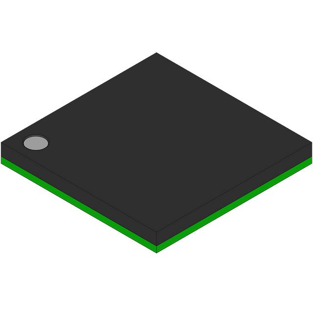
- Part No.:
- LX64B-5F100C
- Manufacturer:
- Lattice Semiconductor Corporation
- Category:
- Specialized ICs
- Package:
- 100-LBGA
- Description:
- CROSSBAR SWITCH, CMOS, PBGA100
- Quantity:
Unit Price:$0
Ext Price:$0
- Payment:

- Shipping:


Product Details
LX64B-5F100C - 64-I/O Programmable Digital Crosspoint
Lattice Semiconductor ispGDX2 device for configurable digital signal routing; 2.5 V B-series, 5.0 ns speed grade, commercial temperature grade and 100-ball fpBGA.
Specifications and lifecycle are based on the official Lattice ispGDX2 family data sheet and PCN09I-10. Confirm the exact order code and controlled drawings before design release.
Overview
LX64B-5F100C is an in-system-programmable digital crosspoint device in Lattice's ispGDX2 family. Its ordering row identifies 64 I/Os, the B-series 2.5 V core-voltage class, a 5.0 ns propagation-delay grade, conventional F100 package and commercial grade. Programmable routing can replace fixed interconnect arrangements in suitable parallel digital interfaces.
Key Advantages
Programmable crosspoint resources support digital signal and bus routing.
The exact ordering row identifies the LX64B 64-I/O option.
The manufacturer lists a 5.0 ns propagation-delay grade for this code.
Routing is configured through the ispGDX2 device architecture.
Feature Summary
The device belongs to Lattice's ispGDX2 programmable bus-switching family.
The ordering table distinguishes its 2.5 V B-series core-voltage class from V-series alternatives.
F100 designates the conventional 100-ball fine-pitch BGA variant.
The terminal C in the exact order code denotes the commercial-grade option.
Package & Footprint
The manufacturer describes F100 as a conventional 100-ball fpBGA; FN100 is a separate lead-free order code. The LCDChip record uses the broader label 100-LBGA. Verify body dimensions, ball pitch, A1 orientation and land pattern against the controlled Lattice package drawing, not the generic catalog label alone.

- Confirm the 100-ball F100 mechanical drawing and A1 orientation.
- Check every ball assignment and required power connection.
- Do not treat F100 and FN100 as identical assembly specifications.
The registered package JPG is currently unavailable on the production site; this detail must not be published until the image is supplied and verified.
Pin Functions
The exact 100-ball fpBGA ball map in the Lattice data sheet controls layout and signal assignment. Functional groups include user I/O, core and I/O-bank supplies, ground, configuration and test connections.
Assign signals according to the selected ispGDX2 routing design and bank rules.
Follow the B-series core-voltage class and each bank's data-sheet requirements.
Connect all designated ground balls as specified by Lattice.
Retain the required configuration and test access in the board design.
This summary is not a ball-by-ball pinout; consult the official 100-ball table before schematic or PCB sign-off.
Key Specifications
| Exact order code | LX64B-5F100C |
|---|---|
| Manufacturer | Lattice Semiconductor Corporation |
| Product family | ispGDX2 |
| Primary function | In-system-programmable digital crosspoint / bus switch |
| User I/O count | 64 |
| Series | LX64B, B-series |
| Core-voltage class | 2.5 V |
| Propagation-delay grade | 5.0 ns, ordering-table designation |
| Manufacturer package code | F100 |
| Package description | 100-ball fine-pitch BGA, conventional variant |
| Catalog package label | 100-LBGA |
| Grade | Commercial (C) |
| Lifecycle evidence | Exact code listed in Lattice PCN09I-10 discontinuance notice |
The speed-grade figure is not a substitute for full timing analysis under actual voltage, loading and temperature conditions.
Replacement Considerations
Lattice PCN09I-10 identifies LX64V-5F100C as a recommended successor to LX64B-5F100C. The V-series voltage requirements differ from the B-series option, so a pin-compatible recommendation is not an automatic electrical replacement. Review rails, I/O-bank levels, timing, programming image, package and qualification before substitution. No internal product link is provided without an exact catalog API match.
Manufacturer Information
The official Lattice ispGDX2 family data sheet contains the exact LX64B-5F100C ordering entry. Lattice PCN09I-10 identifies its lifecycle change and suggested V-series alternative. Use current manufacturer-controlled documentation and drawings for final engineering decisions.
Applications
Programmable paths between compatible digital interfaces in an engineered design.
Configurable crosspoint connections where fixed wiring is unsuitable.
Sustaining assemblies already qualified for this exact discontinued order code.
Quality & Authenticity
For a discontinued device, verify the exact marking and order code, manufacturer documentation, traceability, date and lot codes, ball condition, moisture-sensitive handling and applicable test evidence. Confirm whether the offered unit is the conventional F100 variant; do not infer lead-free status from a generic catalog package name.
FAQ
What does LX64B-5F100C do?
It is a 64-I/O in-system-programmable digital crosspoint device in the Lattice ispGDX2 family.
Which package does this code specify?
F100 is the conventional 100-ball fpBGA manufacturer code; the catalog's 100-LBGA term is broader.
Is LX64V-5F100C a drop-in substitute?
No substitution should be assumed. Lattice recommends it in a PCN, but the voltage requirements require design review.
Can this page be released now?
Not yet. The registered production package image is missing and must be checked before publication.
Engineering Notice
Confirm the official data sheet, PCN, complete ball map, mechanical drawing, electrical conditions and lifecycle requirements before specifying this legacy part or a successor. The missing production package JPG must be resolved and the rendered page rechecked before release.
LX64B-5F100C Information
- Specifications
- Tags
- Product attributes
- Attribute value
- Manufacturer:
- Lattice Semiconductor Corporation
- Series:
- ispGDX2™
- Package/Case:
- 100-LBGA
- Packaging:
- Bulk
- Product Status:
- Active
- Programmable:
- -
- Type:
- Crosspoint Switch
- Applications:
- -
- Mounting Type:
- Surface Mount
- Supplier Device Package:
- 100-FPBGA (11x11)
- Grade:
- -
- Qualification:
- -
- Include Parts
- Popular Search
The following parts include "LX64B-5F100C" in Silicon Labs LX64B-5F100C.
- Part Number
- Manufacturer
- Package
- Description
- CAP200DG-TL Power Integrations 8-SOIC (0.154", 3.90mm Width) IC AUTOMATIC DISCHARGE 8SO
- ATSHA204A-MAHDA-T Microchip Technology 8-UFDFN Exposed Pad IC AUTHENTICATION CHIP 8UDFN
- ATSHA204A-SSHDA-T Microchip Technology 8-SOIC (0.154", 3.90mm Width) IC AUTHENTICATION CHIP 8SOIC
- ATSHA204A-STUCZ-T Microchip Technology TO-236-3, SC-59, SOT-23-3 IC AUTHENTICATION CHIP SOT23-3
- ATECC608B-MAHDA-T Microchip Technology 8-UFDFN Exposed Pad IC AUTHENTICATION CHIP 8UDFN
- ATECC608B-MAHCZ-S Microchip Technology 8-UFDFN Exposed Pad IC AUTHENTICATION CHIP 8UDFN
- ATECC608B-SSHDA-T Microchip Technology 8-SOIC (0.154", 3.90mm Width) IC AUTHENTICATION CHIP 8SOIC
- ATECC608B-MAHDA-S Microchip Technology 8-UFDFN Exposed Pad IC AUTHENTICATION CHIP 8UDFN
- ATECC608A-MAHDA-S Microchip Technology 8-UFDFN Exposed Pad IC AUTHENTICATION CHIP 8UDFN
- ATECC608B-MAVDA-T Microchip Technology 8-UFDFN Exposed Pad IC AUTHENTICATION CHIP 8UDFN
The following parts are popular search parts in Test and Measurement.
Inventory:3,898
Please send an inquiry. Send us your inquiry, and we will respond immediately.


