 Hello! now
 tms@lcdchip.com



Analog Devices Inc. LTC4213CDDB#TRPBF

- Part No.:
- LTC4213CDDB#TRPBF
- Manufacturer:
- Analog Devices Inc.
- Category:
- Specialized ICs
- Package:
- 8-WFDFN Exposed Pad
- Description:
- IC ELECTRONIC CIRC BREAKER 8DFN
- Quantity:
Unit Price:$0
Ext Price:$0
- Payment:

- Shipping:


Product Details
LTC4213CDDB#TRPBF - No-RSENSE Electronic Circuit Breaker
LTC4213CDDB#TRPBF is an Analog Devices electronic circuit breaker controller for an external high-side N-channel MOSFET. The exact C-grade order code is supplied in an eight-lead, 3 mm × 2 mm exposed-pad DFN package on tape and reel and is specified for 0°C to 70°C.
The circuit-breaker threshold senses the MOSFET drain-to-source voltage; current-trip accuracy therefore depends on the selected MOSFET's RDS(ON) and thermal behavior.
Overview
The LTC4213 monitors the voltage between SENSEP and SENSEN across an external N-channel MOSFET, eliminating a discrete series sense resistor. An internal charge pump drives the gate. Separate slow and fast comparators provide two levels of overcurrent protection, while ON controls startup and fault reset and READY indicates an armed, conducting switch.
Key Advantages
The external MOSFET doubles as the sensing element, so a dedicated series resistor is unnecessary.
Slow and fast comparator paths address sustained overloads and severe short circuits.
ISEL chooses among three nominal slow-trip voltage thresholds.
ON enables and resets the breaker; open-drain READY reports the armed state.
Feature Summary
VCC operates from 2.3 V to 6 V; the controlled load path may be 0 V to 6 V.
An internal charge pump supplies nominal 100 µA gate pullup for the external N-channel FET.
ISEL low, floating or tied to VCC sets nominal slow thresholds of 25 mV, 50 mV or 100 mV.
An internal lockout inhibits operation below the bias threshold.
Package & Footprint
LCDChip registers 8-WFDFN Exposed Pad. The manufacturer's exact-order table describes LTC4213CDDB#TRPBF as an eight-lead 3 mm × 2 mm plastic DFN (DDB) with exposed pad and tape-and-reel supply. The exposed pad may be left open or connected to device ground according to the data sheet; use the DDB land pattern, not the TSOT-23 footprint.
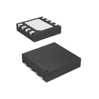
- Confirm DDB orientation and 3 mm × 2 mm body dimensions.
- Route SENSEP and SENSEN to opposite ends of the external MOSFET.
- Check gate-loop layout and fault-current thermal limits.
The expected local JPG is absent and its production URL returns HTTP 404. Keep this draft unpublished until the correct image is restored and inspected.
Pin Functions
For the DDB DFN only: pin 1 READY is an open-drain armed-state output; pin 2 ON controls enable and reset; pin 3 ISEL selects the trip level; pin 4 GND is device ground; pin 5 GATE drives the external N-channel MOSFET; pin 6 SENSEN connects to its source; pin 7 SENSEP connects to its drain; and pin 8 VCC is the 2.3 V to 6 V bias input. Exposed pad 9 may remain open or connect to ground. The TSOT-23 variant has a different pin mapping.
Key Specifications
| Function | No-RSENSE electronic circuit breaker controller |
|---|---|
| Exact order code | LTC4213CDDB#TRPBF |
| Package | Eight-lead 3 mm × 2 mm DDB DFN with exposed pad |
| Supply format | Tape and reel |
| Temperature grade | C grade, 0°C to 70°C |
| Bias supply VCC | 2.3 V to 6 V |
| Controlled load range | 0 V to 6 V |
| Slow-trip nominal thresholds | 25 mV, 50 mV or 100 mV across SENSEP–SENSEN, by ISEL state |
| Fast-trip nominal thresholds | 100 mV, 175 mV or 325 mV for corresponding ISEL states |
| Fast-fault response | 1 µs typical under the manufacturer's stated test conditions |
| Slow-fault response | 16 µs typical under the manufacturer's stated test conditions |
| Gate pullup | 100 µA nominal |
| READY output | Open drain, high impedance when switch is on and breaker armed |
The threshold and timing figures are condition-dependent; use the full min/typ/max electrical tables for design limits.
Replacement Considerations
Do not assume that other LTC4213 grades or packages are interchangeable. The I-grade DDB order code has a wider temperature range, but grade selection, ordering suffix and actual supplied part must be checked. TSOT-23 options use a different footprint and pin assignment. Other circuit breakers can differ in sense method, trip thresholds, gate-drive behavior and reset logic. No unverified internal alternative is linked.
Manufacturer Information
Analog Devices' LTC4213 No RSENSE Electronic Circuit Breaker data sheet Rev. A provides the exact C-grade DDB ordering row, pin functions, operating conditions and protection characteristics. Check the latest controlled revision and package drawing during design release.
Applications
Disconnect a load when the external MOSFET sense voltage exceeds the chosen threshold.
Control an external N-channel FET with status feedback.
Protect low-voltage plug-in load paths during insertion.
Avoid a dedicated series sense resistor where MOSFET-based trip accuracy is acceptable.
Quality & Authenticity
Check device marking, lot traceability, DDB body and pad geometry, and the shipped C-grade order code. Validate the three ISEL configurations, ON reset, READY status, gate discharge and both fault paths on the target board. Characterize the external FET over temperature.
FAQ
Does this device include the power MOSFET?
No. It drives and senses an external N-channel MOSFET.
Is a separate sense resistor required?
No. The controller monitors voltage across the external MOSFET, with trip current dependent on RDS(ON).
What is the exact temperature grade?
The C-grade LTC4213CDDB#TRPBF is specified for 0°C to 70°C.
Why is this detail not published?
The registered package JPG is not available on the production site.
Engineering Notice
Confirm MOSFET RDS(ON) variation, safe operating area, thermal response, trip thresholds, DDB footprint and system fault behavior using the current manufacturer documentation. Restore and visually verify the production package JPG before formal publication.
LTC4213CDDB#TRPBF Information
- Specifications
- Tags
- Product attributes
- Attribute value
- Manufacturer:
- Analog Devices Inc.
- Series:
- -
- Package/Case:
- 8-WFDFN Exposed Pad
- Packaging:
- Tape & Reel (TR)
- Product Status:
- Active
- Programmable:
- Not Verified
- Type:
- Electronic Circuit Breaker
- Applications:
- -
- Mounting Type:
- Surface Mount
- Supplier Device Package:
- 8-DFN (3x2)
- Grade:
- -
- Qualification:
- -
- Include Parts
- Popular Search
The following parts include "LTC4213CDDB#TRPBF" in Silicon Labs LTC4213CDDB#TRPBF.
- Part Number
- Manufacturer
- Package
- Description
- CAP200DG-TL Power Integrations 8-SOIC (0.154", 3.90mm Width) IC AUTOMATIC DISCHARGE 8SO
- ATSHA204A-MAHDA-T Microchip Technology 8-UFDFN Exposed Pad IC AUTHENTICATION CHIP 8UDFN
- ATSHA204A-SSHDA-T Microchip Technology 8-SOIC (0.154", 3.90mm Width) IC AUTHENTICATION CHIP 8SOIC
- ATSHA204A-STUCZ-T Microchip Technology TO-236-3, SC-59, SOT-23-3 IC AUTHENTICATION CHIP SOT23-3
- ATECC608B-MAHDA-T Microchip Technology 8-UFDFN Exposed Pad IC AUTHENTICATION CHIP 8UDFN
- ATECC608B-MAHCZ-S Microchip Technology 8-UFDFN Exposed Pad IC AUTHENTICATION CHIP 8UDFN
- ATECC608B-SSHDA-T Microchip Technology 8-SOIC (0.154", 3.90mm Width) IC AUTHENTICATION CHIP 8SOIC
- ATECC608B-MAHDA-S Microchip Technology 8-UFDFN Exposed Pad IC AUTHENTICATION CHIP 8UDFN
- ATECC608A-MAHDA-S Microchip Technology 8-UFDFN Exposed Pad IC AUTHENTICATION CHIP 8UDFN
- ATECC608B-MAVDA-T Microchip Technology 8-UFDFN Exposed Pad IC AUTHENTICATION CHIP 8UDFN
The following parts are popular search parts in Test and Measurement.
Inventory:4,917
Please send an inquiry. Send us your inquiry, and we will respond immediately.


