 Hello! now
 tms@lcdchip.com



Intersil HSP45240JC-33
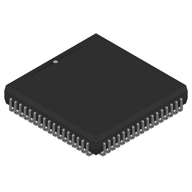
- Part No.:
- HSP45240JC-33
- Manufacturer:
- Intersil
- Category:
- Specialized ICs
- Package:
- 68-LCC (J-Lead)
- Description:
- IC ADDRESS SEQUENCER 68PLCC
- Quantity:
Unit Price:$0
Ext Price:$0
- Payment:

- Shipping:


Product Details
HSP45240JC-33 - 33 MHz Address Sequencer
HSP45240JC-33 is Intersil's 24-bit address sequencer in a 68-lead PLCC package. The exact ordering row specifies commercial 0 to 70 °C operation, and the -33 timing column specifies a 30 ns minimum clock period.
This legacy IC needs its original programming model and PLCC pinout checked against the target design.
Overview
The HSP45240 generates address sequences for block-oriented signal and image processing. A 24-by-24 crosspoint switch maps internal address bits to 24 output pins; the device can alternatively serve as two independent 12-bit sequencers. Its processor interface programs the sequence and control settings.
Key Advantages
- Block-oriented 24-bit address generation.
- Two independent 12-bit sequencing option.
- 24-by-24 crosspoint output mapping for transformations such as bit reversal.
- Programmable delay on 12 address outputs for pipeline alignment.
- Processor programming interface and multi-chip synchronization signals.
Feature Summary
Start circuitry feeds the sequence generator and crosspoint switch. The upper 12 output bits pass through a register; the lower 12 can pass through selectable delay stages. STARTIN and STARTOUT support cascaded devices. ADDVAL, BLOCKDONE, DONE and BUSY report sequence state; separate output-enable controls gate the two output banks.
Package & Footprint
The manufacturer's exact-order table lists HSP45240JC-33 in a 68-lead PLCC with package drawing N68.95. LCDChip records 68-LCC (J-Lead) and its registry maps this to /upload/package/68-LCC.jpg. Confirm lead orientation, pin-one marker and mechanical dimensions from N68.95 before using any generic footprint.

- Match N68.95 mechanical drawing.
- Verify socket or land pattern and pin one.
- Account for all supply and ground leads.
The registered JPG is missing locally and must be restored and reviewed before publication.
Pin Functions
The manufacturer's PLCC pin table places OEL at pin 29, DLYBLK at pin 30 and STARTIN at pin 31. STARTOUT, ADDVAL, BUSY, BLOCKDONE and DONE are on pins 32, 33, 35, 36 and 37. OUT0-23 is the 24-bit address output bank. The D0-6, CS, A0 and WR signals form the processor control interface; OEH and OEL independently enable the upper and lower output groups.
STARTIN, STARTOUT and DLYBLK.
OUT0-23 and two output-enable inputs.
ADDVAL, BUSY, BLOCKDONE and DONE.
D0-6, CS, A0 and WR.
Use the complete numbered PLCC table for schematic release; this is a functional summary.
Key Specifications
| Function | Programmable address sequencer |
|---|---|
| Exact ordering code | HSP45240JC-33 |
| Speed grade | -33, 33 MHz |
| Minimum clock period | 30 ns for -33 grade |
| Supply test condition | 5.0 V ±5% in AC table |
| Operating temperature | 0 to 70 °C, ordering table |
| Address width | 24 bits, or two 12-bit sequences |
| Crosspoint switch | 24-by-24 |
| Programmable output delay | 12 output bits |
| Package | 68-lead PLCC, N68.95 |
Use manufacturer timing conditions and board loading for final limits.
Replacement Considerations
The HSP45240JC-50 is a faster grade listed in the same family but is not an automatic drop-in: verify timing, power, package revision and qualification. Other address generators may differ in programming registers, crosspoint behavior, output delay or synchronization. No internal alternative link is shown without exact database and engineering verification.
Manufacturer Information
The Intersil HSP45240 data sheet, FN2489.4, July 2004, is hosted by Renesas and includes the exact HSP45240JC-33 ordering entry, 68-lead PLCC pin descriptions, architecture and -33 AC timing column. Confirm document revision and device markings for legacy inventory.
Applications
- One- and two-dimensional filtering address generation.
- FFT address ordering and bit-reversal mapping.
- Pan, zoom and image-address transforms.
- Matrix operations and legacy DSP boards.
Quality & Authenticity
Verify the full JC-33 marking, 68-lead package, lot traceability, storage and ESD handling. Compare the seller's offered quantity and date code with purchase records. Electrical compatibility depends on timing, interface programming and the original board.
FAQ
Is the -33 part rated for 50 MHz?
No. Its AC column is the 33 MHz grade with a 30 ns minimum clock period.
Can the outputs be used as two sequencers?
Yes. The data sheet describes two independent 12-bit sequencing operation.
Is the 68-LCC image available?
No. The registered JPG is currently missing locally.
Is current stock and a complete price ladder verified?
No. Exact-code listings do not establish a dependable live full ladder for release.
Engineering Notice
Review N68.95 mechanical details, complete pinout, 5 V supply/decoupling, -33 clock timing, processor-write timing, output loading and synchronization before design release. Missing package JPG and unverified current exact-code stock and tier prices block automatic publication.
HSP45240JC-33 Information
- Specifications
- Tags
- Product attributes
- Attribute value
- Manufacturer:
- Intersil
- Series:
- -
- Package/Case:
- 68-LCC (J-Lead)
- Packaging:
- Bulk
- Product Status:
- Active
- Programmable:
- Not Verified
- Type:
- Address Sequencer
- Applications:
- -
- Mounting Type:
- Surface Mount
- Supplier Device Package:
- 68-PLCC (24.23x24.23)
- Grade:
- -
- Qualification:
- -
- Include Parts
- Popular Search
The following parts include "HSP45240JC-33" in Silicon Labs HSP45240JC-33.
- Part Number
- Manufacturer
- Package
- Description
- CAP200DG-TL Power Integrations 8-SOIC (0.154", 3.90mm Width) IC AUTOMATIC DISCHARGE 8SO
- ATSHA204A-MAHDA-T Microchip Technology 8-UFDFN Exposed Pad IC AUTHENTICATION CHIP 8UDFN
- ATSHA204A-SSHDA-T Microchip Technology 8-SOIC (0.154", 3.90mm Width) IC AUTHENTICATION CHIP 8SOIC
- ATSHA204A-STUCZ-T Microchip Technology TO-236-3, SC-59, SOT-23-3 IC AUTHENTICATION CHIP SOT23-3
- ATECC608B-MAHDA-T Microchip Technology 8-UFDFN Exposed Pad IC AUTHENTICATION CHIP 8UDFN
- ATECC608B-MAHCZ-S Microchip Technology 8-UFDFN Exposed Pad IC AUTHENTICATION CHIP 8UDFN
- ATECC608B-SSHDA-T Microchip Technology 8-SOIC (0.154", 3.90mm Width) IC AUTHENTICATION CHIP 8SOIC
- ATECC608B-MAHDA-S Microchip Technology 8-UFDFN Exposed Pad IC AUTHENTICATION CHIP 8UDFN
- ATECC608A-MAHDA-S Microchip Technology 8-UFDFN Exposed Pad IC AUTHENTICATION CHIP 8UDFN
- ATECC608B-MAVDA-T Microchip Technology 8-UFDFN Exposed Pad IC AUTHENTICATION CHIP 8UDFN
The following parts are popular search parts in Test and Measurement.
Inventory:1,929
Please send an inquiry. Send us your inquiry, and we will respond immediately.


