 Hello! now
 tms@lcdchip.com



Harris Corporation HSP45240GC-50
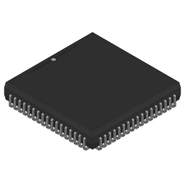
- Part No.:
- HSP45240GC-50
- Manufacturer:
- Harris Corporation
- Category:
- Specialized ICs
- Package:
- 68-BCPGA
- Description:
- IC ADDRESS SEQUENCER 68CPGA
- Quantity:
Unit Price:$0
Ext Price:$0
- Payment:

- Shipping:


Product Details
HSP45240GC-50 - 50 MHz Address Sequencer
HSP45240GC-50 is the Harris/Intersil 24-bit address sequencer in a 68-lead pin-grid array (PGA), G68.A drawing, with a -50 clock grade. It supports block-oriented addressing and programmable output mapping for digital signal-processing memory systems.
Check the original package drawing and the actual device marking before board assembly.
Overview
The HSP45240 generates address sequences for FFT processing, one- and two-dimensional filtering, matrix operations and image manipulation. Its 24-by-24 crosspoint switch maps internally generated address bits to 24 output lines. The device can instead be configured as two independent 12-bit sequencers.
Key Advantages
Flexible address order
A 24-by-24 crosspoint switch supports output bit mapping, including FFT bit-reverse patterns.
Two operating configurations
Use one 24-bit sequencer or two independent 12-bit sequencers as the application requires.
Pipeline alignment
Programmable delays are available on 12 address outputs.
System control
A processor interface and synchronization signals support configuration and multichip designs.
Feature Summary
Sequence generation
Block-oriented address generation across a 24-bit output span.
Output control
Separate enable inputs for high and low output groups, with status and completion signals.
Timing
The manufacturer lists a DC-to-50 MHz clock range for the -50 grade.
Logic family
Fully static CMOS design; verify the original DC and AC conditions for the intended load.
Package & Footprint
The original ordering table identifies HSP45240GC-50 as a 68-lead PGA, package drawing G68.A. The catalog calls it 68-BCPGA. This is not the JC 68-lead PLCC variant; their footprints must not be interchanged. The local 68-BCPGA registration mapping has not been independently confirmed and its JPG is absent.

- Use the PGA bottom-view drawing, not the PLCC top view.
- Confirm the G68.A mechanical drawing and pin-one orientation.
- Inspect the supplied lot and verify socket or board-hole compatibility.
The package JPG and local registry match must be completed before publication.
Pin Functions
The manufacturer data sheet shows a separate 68-pin PGA bottom-view diagram. Functional groups are summarized here; use that original drawing for physical pin coordinates.
Processor interface
D0-D6, A0, WR and active-low CS program the configuration registers.
Timing and reset
CLK is the sequencer clock; active-low RST initializes operation.
Address outputs
OUT0-OUT23 present mapped address bits; OEH and OEL enable output groups.
Sequencing and status
STARTIN, STARTOUT, DLYBLK, ADDVAL, BUSY, DONE and BLOCKDONE coordinate sequence progress.
Do not infer PGA coordinates from the PLCC pin numbers printed beside the functional descriptions.
Key Specifications
| Exact order code | HSP45240GC-50 |
|---|---|
| Function | Address sequencer |
| Primary width | 24-bit, block-oriented |
| Alternate configuration | Two independent 12-bit sequencers |
| Crosspoint mapping | 24 by 24 |
| Delayed outputs | Programmable delay on 12 outputs |
| Clock grade | DC to 50 MHz for -50 version |
| Package | 68-lead PGA, manufacturer drawing G68.A |
| Ordering temperature | 0 to 70 degrees C |
| Processor interface | D0-D6, CS, A0 and WR |
| Output loading feature | 100 pF drive stated in manufacturer feature list |
| Process | Fully static CMOS |
Apply the data sheet's voltage, loading and temperature conditions when using timing or electrical limits; the ordering row alone does not qualify an individual stored lot.
Replacement Considerations
The HSP45240GC-33 and GC-40 are documented PGA speed grades of the same family, but their timing limits differ from the GC-50. The JC-50 has a PLCC footprint and is not a board-level substitute for this PGA device. Verify clock budget, pinout, output loading, temperature grade and firmware configuration before considering any change. No unverified internal product link is supplied.
Manufacturer Information
Harris/Intersil authored the HSP45240 Address Sequencer data sheet. Its September 1997 ordering table lists HSP45240GC-50, 0 to 70 degrees C and 68-lead PGA drawing G68.A; its PGA diagram and pin descriptions are the basis for the functional groups above. Renesas maintains a later Intersil-branded family document, but exact package and speed selection should follow the controlled ordering record for the supplied lot.
Applications
Digital filtering
Address generation for one- and two-dimensional filtering pipelines.
FFT processing
Mapped address ordering, including bit-reverse patterns.
Image manipulation
Pan, zoom and matrix address sequencing in legacy signal-processing systems.
System maintenance
Replacement assessment for qualified equipment already designed around the PGA variant.
Quality & Authenticity
Check the full GC-50 marking, date and lot code, PGA pin condition and traceability to the original specification. Verify solderability or socket condition for long-stored inventory. The listing is not a claim of new production, electrical retest or any certification.
FAQ
Can the JC-50 replace this device?
Not without a board redesign: JC-50 is the PLCC package, whereas GC-50 is PGA.
Does -50 identify 50 MHz?
Yes. The original ordering table and clock-grade specifications identify the -50 speed grade.
Can the output sequence be remapped?
Yes. The 24-by-24 crosspoint switch remaps generated address bits to outputs.
Is package artwork ready?
No. The candidate 68-BCPGA JPG is absent locally and the register mapping still needs verification.
Engineering Notice
Keep this detail under review until the exact G68.A mechanical drawing, local 68-BCPGA registry mapping, package JPG and supplied lot are checked. Reconcile current distributor stock and tier pricing before any commercial update. Do not publish while the image or verification gates remain open.
HSP45240GC-50 Information
- Specifications
- Tags
- Product attributes
- Attribute value
- Manufacturer:
- Harris Corporation
- Series:
- -
- Package/Case:
- 68-BCPGA
- Packaging:
- Bulk
- Product Status:
- Active
- Programmable:
- Not Verified
- Type:
- Address Sequencer
- Applications:
- -
- Mounting Type:
- Through Hole
- Supplier Device Package:
- 68-CPGA (29.47x29.47)
- Grade:
- -
- Qualification:
- -
- Include Parts
- Popular Search
The following parts include "HSP45240GC-50" in Silicon Labs HSP45240GC-50.
- Part Number
- Manufacturer
- Package
- Description
- CAP200DG-TL Power Integrations 8-SOIC (0.154", 3.90mm Width) IC AUTOMATIC DISCHARGE 8SO
- ATSHA204A-MAHDA-T Microchip Technology 8-UFDFN Exposed Pad IC AUTHENTICATION CHIP 8UDFN
- ATSHA204A-SSHDA-T Microchip Technology 8-SOIC (0.154", 3.90mm Width) IC AUTHENTICATION CHIP 8SOIC
- ATSHA204A-STUCZ-T Microchip Technology TO-236-3, SC-59, SOT-23-3 IC AUTHENTICATION CHIP SOT23-3
- ATECC608B-MAHDA-T Microchip Technology 8-UFDFN Exposed Pad IC AUTHENTICATION CHIP 8UDFN
- ATECC608B-MAHCZ-S Microchip Technology 8-UFDFN Exposed Pad IC AUTHENTICATION CHIP 8UDFN
- ATECC608B-SSHDA-T Microchip Technology 8-SOIC (0.154", 3.90mm Width) IC AUTHENTICATION CHIP 8SOIC
- ATECC608B-MAHDA-S Microchip Technology 8-UFDFN Exposed Pad IC AUTHENTICATION CHIP 8UDFN
- ATECC608A-MAHDA-S Microchip Technology 8-UFDFN Exposed Pad IC AUTHENTICATION CHIP 8UDFN
- ATECC608B-MAVDA-T Microchip Technology 8-UFDFN Exposed Pad IC AUTHENTICATION CHIP 8UDFN
The following parts are popular search parts in Test and Measurement.
Inventory:1,416
Please send an inquiry. Send us your inquiry, and we will respond immediately.


