 Hello! now
 tms@lcdchip.com



Harris Corporation HSP45240GC-40
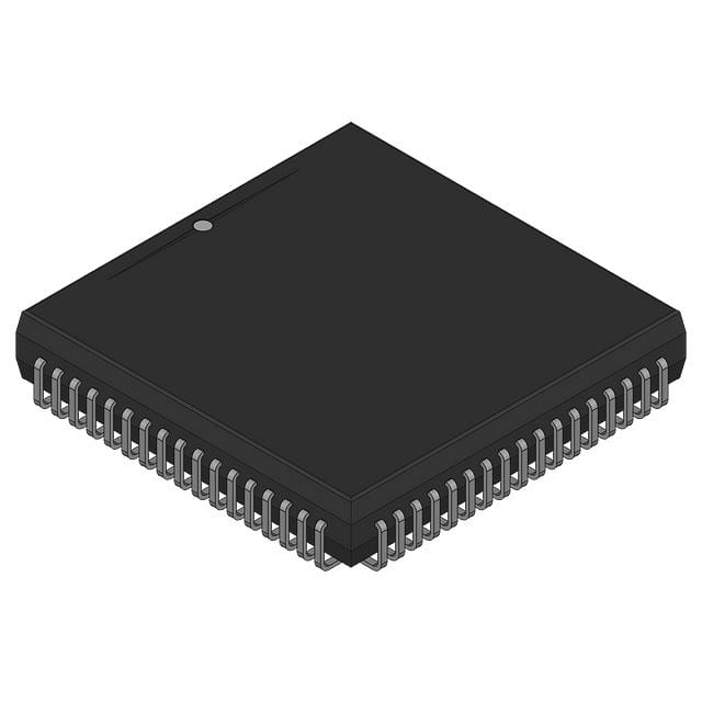
- Part No.:
- HSP45240GC-40
- Manufacturer:
- Harris Corporation
- Category:
- Specialized ICs
- Package:
- 68-BCPGA
- Description:
- IC ADDRESS SEQUENCER 68CPGA
- Quantity:
Unit Price:$0
Ext Price:$0
- Payment:

- Shipping:


Product Details
HSP45240GC-40 - 40 MHz Address Sequencer
Harris Corporation HSP45240GC-40 is a 24-bit programmable address sequencer in a 68-lead ceramic PGA, package drawing G68.A. The manufacturer-authored Intersil HSP45240 ordering table identifies this exact 0 to +70 C, -40 speed-grade variant.
Use the GC PGA bottom-view coordinate map and -40 timing column, not the JC PLCC numbered pinout or the faster -50 grade.
Overview
The HSP45240 creates block-oriented memory-address sequences for DSP and image-processing work. A 24-by-24 crosspoint switch remaps output address bits for patterns such as FFT bit reversal. The same device can be configured as two independent 12-bit sequencers, with programmable delay on twelve outputs and a processor interface for setup.
Key Advantages
Twenty-four-bit block sequencing for memory-oriented algorithms.
Two independent twelve-bit address streams when configured.
Twenty-four-by-twenty-four mapping supports nonsequential output patterns.
Programmable delay on twelve address outputs helps align stages.
Feature Summary
D0-D6, CS, A0 and WR form a microprocessor configuration interface.
STARTIN and STARTOUT support coordinated sequencing across devices.
ADDVAL, BUSY, BLOCKDONE and DONE report sequence progress.
OEH and OEL control upper and lower output groups separately.
Package & Footprint
The 1997 manufacturer-authored ordering table specifies HSP45240GC-40 as a 68-lead PGA, drawing G68.A. The catalog's 68-BCPGA matches the local registered normalized package name, recorded in workbook row 713 in the immediately preceding batch. The PGA bottom view differs from the PLCC top view; verify ceramic body size, keying, pin grid and socket against G68.A and the shipped lot.

- Match G68.A grid and bottom-view orientation.
- Check socket/key and pin pitch.
- Inspect ceramic body and pin condition.
The registered 68-BCPGA JPG is absent locally; keep the page unpublished.
Pin Functions
The manufacturer's PGA bottom view identifies D0-D6, CS, A0 and WR for programming; CLK and RST for timing and reset; STARTIN, STARTOUT and DLYBLK for sequence control; ADDVAL, BUSY, BLOCKDONE and DONE for status; and OUT0-OUT23 with OEH/OEL for address outputs. Use the letter-number PGA grid in the controlled diagram. A PLCC pin number cannot be transferred to this package.
D0-D6, CS, A0 and WR.
CLK, RST, STARTIN, STARTOUT and DLYBLK.
ADDVAL, BUSY, BLOCKDONE and DONE.
OUT0-OUT23 with OEH and OEL.
Confirm all G68.A coordinates and the supplied lot's orientation before schematic release.
Key Specifications
| Exact order code | HSP45240GC-40 |
|---|---|
| Original maker | Harris Corporation / later Intersil documentation |
| Function | Programmable address sequencer |
| Speed grade | -40, 40 MHz class |
| Minimum clock period | 25 ns, -40 AC column, VCC 5.0 V ±5%, TA 0 to +70 C |
| Minimum clock high/low | 10 ns each under the same -40 AC conditions |
| Address width | 24 bits or two 12-bit streams |
| Crosspoint switch | 24-by-24 |
| Programmable output delay | 12 output bits |
| Supply | 5.0 V nominal family, check full DC limits |
| Temperature range | 0 to +70 C exact ordering row |
| Package | 68-lead PGA G68.A; catalog 68-BCPGA |
Timing limits apply only under the manufacturer's stated loading and test conditions.
Replacement Considerations
No LCDChip internal alternate is linked or approved. Harris listed GC-33 and GC-50 PGA speed grades and JC-40 PLCC. GC-33 is slower; GC-50 needs electrical and procurement checks; JC-40 has a different package. Validate programming behavior, reset, output loading, clock margin, G68.A grid and temperature grade before any substitution.
Manufacturer Information
Harris' historical product guide and the 1997 Intersil HSP45240 data sheet list exact GC-40 in a commercial 68-lead PGA, G68.A. The later Renesas-hosted family data sheet includes -40 electrical timing but presents the JC PLCC package in its reduced ordering table. Keep the original GC package document with the device's traceability records.
Applications
Bit reversal and mapped memory traversal.
Pan and zoom address generation.
One- and two-dimensional data-block sequencing.
Coordinated reads and writes in legacy DSP systems.
Quality & Authenticity
Check the exact Harris GC-40 marking, date/lot code, original ceramic PGA and pin condition. Catalog stock and base price are separate commercial fields. Indexed exact-code sellers disagree on stock and quantity pricing; secure a dated authorized quote and confirm lot provenance before updating inventory terms or publishing.
FAQ
Is the -40 grade the 50 MHz family maximum?
No. Its AC column specifies a 25 ns minimum clock period, corresponding to the 40 MHz class.
Is GC-40 pin-compatible with JC-40?
No direct package substitution is established; GC is PGA and JC is PLCC.
Can it generate two address streams?
Yes, family documentation describes two independent 12-bit sequencers.
Is the package image ready?
No. The registered 68-BCPGA JPG is missing locally.
Engineering Notice
Keep this item in manual review. Restore the 68-BCPGA JPG, verify G68.A coordinates and the supplied lot, reconcile exact-code authorized stock and tier pricing, and repeat database and rendered-page checks. No release or drop-in substitution is approved.
HSP45240GC-40 Information
- Specifications
- Tags
- Product attributes
- Attribute value
- Manufacturer:
- Harris Corporation
- Series:
- -
- Package/Case:
- 68-BCPGA
- Packaging:
- Bulk
- Product Status:
- Active
- Programmable:
- Not Verified
- Type:
- Address Sequencer
- Applications:
- -
- Mounting Type:
- Through Hole
- Supplier Device Package:
- 68-CPGA (29.47x29.47)
- Grade:
- -
- Qualification:
- -
- Include Parts
- Popular Search
The following parts include "HSP45240GC-40" in Silicon Labs HSP45240GC-40.
- Part Number
- Manufacturer
- Package
- Description
- CAP200DG-TL Power Integrations 8-SOIC (0.154", 3.90mm Width) IC AUTOMATIC DISCHARGE 8SO
- ATSHA204A-MAHDA-T Microchip Technology 8-UFDFN Exposed Pad IC AUTHENTICATION CHIP 8UDFN
- ATSHA204A-SSHDA-T Microchip Technology 8-SOIC (0.154", 3.90mm Width) IC AUTHENTICATION CHIP 8SOIC
- ATSHA204A-STUCZ-T Microchip Technology TO-236-3, SC-59, SOT-23-3 IC AUTHENTICATION CHIP SOT23-3
- ATECC608B-MAHDA-T Microchip Technology 8-UFDFN Exposed Pad IC AUTHENTICATION CHIP 8UDFN
- ATECC608B-MAHCZ-S Microchip Technology 8-UFDFN Exposed Pad IC AUTHENTICATION CHIP 8UDFN
- ATECC608B-SSHDA-T Microchip Technology 8-SOIC (0.154", 3.90mm Width) IC AUTHENTICATION CHIP 8SOIC
- ATECC608B-MAHDA-S Microchip Technology 8-UFDFN Exposed Pad IC AUTHENTICATION CHIP 8UDFN
- ATECC608A-MAHDA-S Microchip Technology 8-UFDFN Exposed Pad IC AUTHENTICATION CHIP 8UDFN
- ATECC608B-MAVDA-T Microchip Technology 8-UFDFN Exposed Pad IC AUTHENTICATION CHIP 8UDFN
The following parts are popular search parts in Test and Measurement.
Inventory:889
Please send an inquiry. Send us your inquiry, and we will respond immediately.


