 Hello! now
 tms@lcdchip.com



Fairchild Semiconductor FSSD06UMX
- Part No.:
- FSSD06UMX
- Manufacturer:
- Fairchild Semiconductor
- Category:
- Specialized ICs
- Package:
- 24-UFQFN
- Description:
- DIFFERENTIAL MULTIPLEXER, 4 CHAN
- Quantity:
Unit Price:$0
Ext Price:$0
- Payment:

- Shipping:


Product Details
FSSD06UMX - SD/SDIO and MMC Two-Port Multiplexer
A dual-card-port SD/SDIO/MMC signal multiplexer with bidirectional data and command paths, buffered clock routing, independent card-port supplies, and high-impedance disable control.
The exact FSSD06UMX code and 24-lead ultrathin molded leadless package are documented by Fairchild/onsemi.
Overview
FSSD06UMX routes one host SD/SDIO or MMC interface to either of two card-side ports. DAT[3:0] and CMD are bidirectional paths, while CLK is distributed through a unidirectional buffered path. Separate VDDC1 and VDDC2 rails support card-port voltage domains, and VDDH supplies the host-side interface.
Key Advantages
One host interface can be switched between two SD/SDIO/MMC connections.
CMD and four-bit DAT buses transfer in either direction as required by the protocol.
VDDH, VDDC1, and VDDC2 accommodate host and card-side voltage domains described by the datasheet.
Active-high disable places signal ports in high impedance while inactive clock outputs are pulled high internally.
Feature Summary
Package & Footprint
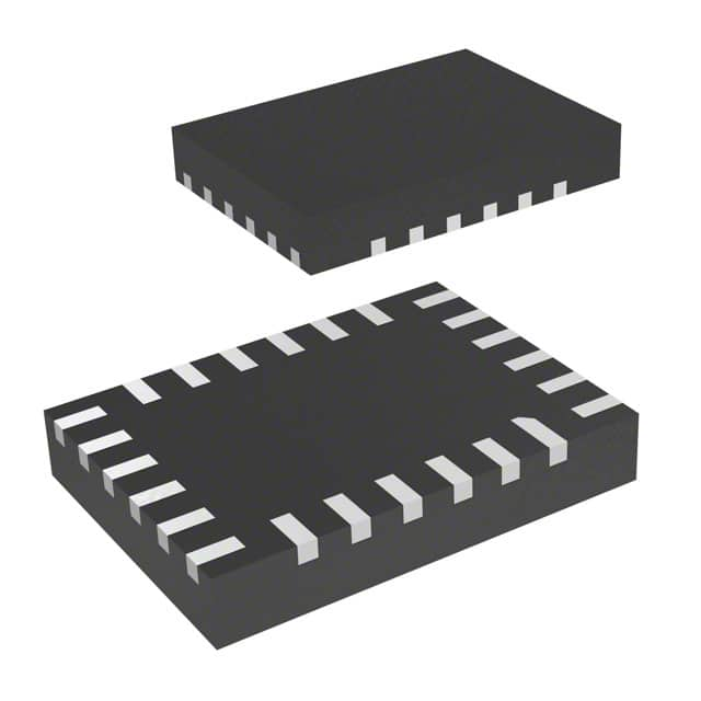
FSSD06UMX uses a 24-lead ultrathin molded leadless package (UMLP). The site registry lists the original product package as 24-UFQFN.

- Use the official UMLP land pattern and pin-one orientation.
- Keep SD clock paths short and controlled.
- Place decoupling close to VDDH, VDDC1, and VDDC2.
- Verify escape routing and solder-mask clearances for the leadless footprint.
The expected production JPG is not currently available; publication must wait for image verification.
Signal Groups
VDDH powers the host ASIC interface domain.
VDDC1 and VDDC2 power the two peripheral-card interface domains.
/OE is active low; S selects card port 1 or 2.
DAT[3:0], CMD, and CLK connect to the host interface.
1DAT[3:0], 1CMD, and 1CLK connect to the first card interface.
2DAT[3:0], 2CMD, and 2CLK connect to the second card interface.
When /OE is high, all signal ports are high impedance and both card clock outputs are held high through internal pull-ups.
Key Specifications
| Ordering code | FSSD06UMX |
|---|---|
| Function | SD/SDIO/MMC two-port multiplexer |
| Data bus | Four bidirectional data lines |
| Command path | Bidirectional |
| Clock path | Unidirectional buffered |
| Host supply | VDDH |
| Card supplies | VDDC1 and VDDC2 |
| Operating temperature | -40 °C to +85 °C |
| Package | 24-lead ultrathin molded leadless package (UMLP) |
| Packing | Tape and reel |
Use the official datasheet for guaranteed voltage ranges, resistance, capacitance, propagation delay, leakage, and timing limits.
Replacement Considerations
No drop-in replacement is asserted. Compare supply-domain ranges, SD/SDIO/MMC signaling direction, clock buffering, internal pull-ups, on-resistance, bandwidth, off isolation, control truth table, power-off behavior, UMLP footprint, and pin assignment.
Manufacturer Information
FSSD06 was introduced by Fairchild Semiconductor and is now supported through onsemi documentation. Primary source: the official FSSD06 datasheet.
Applications
Quality & Authenticity
Verify the FSSD06UMX ordering code, package marking, 24-lead UMLP geometry, pin-one mark, reel label, lot/date code, moisture handling, solderability, and traceability. Inspect the leadless underside for oxidation, reballing, residue, or mechanical damage.
FAQ
It switches four SD data lines, the command line, and the clock path between one host and either of two card ports.
The signal ports enter high impedance while the two card-side clock outputs are pulled high internally.
VDDH supplies the host domain; VDDC1 and VDDC2 supply the two card-port domains.
Engineering Notice
This page is an engineering selection aid. Validate the latest official datasheet, package drawing, voltage-domain sequencing, SD timing, signal integrity, and production footprint before release.
FSSD06UMX Information
- Specifications
- Tags
- Product attributes
- Attribute value
- Manufacturer:
- Fairchild Semiconductor
- Series:
- -
- Package/Case:
- 24-UFQFN
- Packaging:
- Bulk
- Product Status:
- Active
- Programmable:
- Not Verified
- Type:
- Multiplexer
- Applications:
- Cell Phones, Digital Cameras, Media Players
- Mounting Type:
- Surface Mount
- Supplier Device Package:
- 24-UMLP (2.5x3.4)
- Grade:
- -
- Qualification:
- -
- Include Parts
- Popular Search
The following parts include "FSSD06UMX" in Silicon Labs FSSD06UMX.
- Part Number
- Manufacturer
- Package
- Description
- CAP200DG-TL Power Integrations 8-SOIC (0.154", 3.90mm Width) IC AUTOMATIC DISCHARGE 8SO
- ATSHA204A-MAHDA-T Microchip Technology 8-UFDFN Exposed Pad IC AUTHENTICATION CHIP 8UDFN
- ATSHA204A-SSHDA-T Microchip Technology 8-SOIC (0.154", 3.90mm Width) IC AUTHENTICATION CHIP 8SOIC
- ATSHA204A-STUCZ-T Microchip Technology TO-236-3, SC-59, SOT-23-3 IC AUTHENTICATION CHIP SOT23-3
- ATECC608B-MAHDA-T Microchip Technology 8-UFDFN Exposed Pad IC AUTHENTICATION CHIP 8UDFN
- ATECC608B-MAHCZ-S Microchip Technology 8-UFDFN Exposed Pad IC AUTHENTICATION CHIP 8UDFN
- ATECC608B-SSHDA-T Microchip Technology 8-SOIC (0.154", 3.90mm Width) IC AUTHENTICATION CHIP 8SOIC
- ATECC608B-MAHDA-S Microchip Technology 8-UFDFN Exposed Pad IC AUTHENTICATION CHIP 8UDFN
- ATECC608A-MAHDA-S Microchip Technology 8-UFDFN Exposed Pad IC AUTHENTICATION CHIP 8UDFN
- ATECC608B-MAVDA-T Microchip Technology 8-UFDFN Exposed Pad IC AUTHENTICATION CHIP 8UDFN
The following parts are popular search parts in Test and Measurement.
Inventory:271,635
Please send an inquiry. Send us your inquiry, and we will respond immediately.


