 Hello! now
 tms@lcdchip.com



Analog Devices Inc./Maxim Integrated DS2188SN+
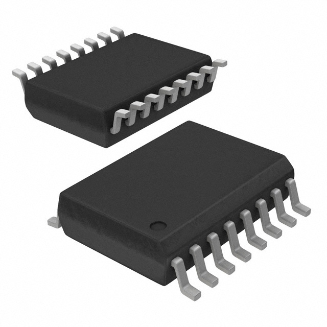
- Part No.:
- DS2188SN+
- Manufacturer:
- Analog Devices Inc./Maxim Integrated
- Category:
- Specialized ICs
- Package:
- 16-SOIC (0.295", 7.50mm Width)
- Description:
- IC ATTEN JTR T1/CEPT IND 16-SOIC
- Quantity:
Unit Price:$0
Ext Price:$0
- Payment:

- Shipping:


Product Details
DS2188SN+ - T1/CEPT Jitter Attenuator
The Dallas Semiconductor DS2188SN+ attenuates clock and data jitter on T1 and CEPT receive paths. It combines a selectable two-bit-wide elastic buffer with a crystal-controlled digital phase-locked loop in a 16-pin SOIC package.
Analog Devices identifies this legacy device as obsolete. The manufacturer data sheet explicitly lists the DS2188SN base code as the industrial-temperature 16-pin SOIC option; verify the additional plus suffix against the physical lot.
Overview
Incoming bipolar receive data enters RPOS and RNEG with RCLK. The DS2188SN+ writes these signals into an elastic buffer and produces dejittered RRPOS, RRNEG and RRCLK outputs. An external crystal provides the reference for the internal timing loop. This function suits maintenance of timing quality in legacy T1 and CEPT equipment, but it is not a complete line transceiver.
Key Benefits
- Attenuates received clock and data jitter in a single IC.
- Supports 1.544 MHz T1 and 2.048 MHz CEPT clock environments.
- Offers 128-bit or 32-bit buffer-depth selection to balance jitter tolerance and delay.
- Provides a bypass control for diagnostics or system-level timing selection.
- Exposes buffer-limit indication for excessive input jitter conditions.
Functional Features
The buffer is 128 x 2 bits in its standard configuration. BDS selects the shorter 32-bit mode. A 6.176 MHz crystal is specified for T1 and an 8.192 MHz crystal for CEPT. The loop averages incoming timing while reducing jitter; DJA high bypasses attenuation. A negative transition on RST recenters the buffer and can disturb data in transit. BL indicates operation near a buffer limit.
Package & Footprint
The manufacturer's DS2188S/SN mechanical drawing describes a 16-pin SOIC body about 7.37 to 7.65 mm wide with 1.27 mm lead pitch. The catalog calls this a 16-SOIC, 0.295-inch-wide package. The existing package registry's plain 16-SOIC entry instead describes a 0.154-inch-wide body, so it is not a verified footprint match. The registered wide-body options describe exposed-pad, PowerSOIC, BSSOP or module variants and must not be substituted. A dedicated wide-body SOIC package entry and verified JPG are required.

- Use the manufacturer drawing for body, lead and land-pattern dimensions.
- Confirm pin-one orientation and board clearance.
- Place crystal and supply bypass components close to the specified pins.
The expected dedicated wide-body package JPG is absent; this draft is not publishable.
Pin Functions
Input group: RPOS pin 2, RNEG pin 3 and RCLK pin 4. Output group: RRCLK pin 13, RRNEG pin 14 and RRPOS pin 15. Control: DJA pin 1, BDS pin 5, TEST pin 6, BL pin 11 and RST pin 12. Crystal connections are XTAL1 pin 9 and XTAL2 pin 10, with XTAL OUT pin 7. VSS is pin 8 and VDD is pin 16. Tie TEST low for normal operation as the data sheet instructs.
Key Specifications
| Function | T1/CEPT clock and data jitter attenuator |
|---|---|
| Catalog order code | DS2188SN+ |
| T1 input clock | 1.544 MHz nominal |
| CEPT input clock | 2.048 MHz nominal |
| T1 crystal | 6.176 MHz |
| CEPT crystal | 8.192 MHz |
| Buffer depth | 128 or 32 bits, BDS-selectable |
| Input jitter capacity | Up to 120 UIpp in 128-bit mode; 28 UIpp in 32-bit mode |
| Supply | Single 5 V nominal |
| Temperature | -40 to +85 degrees C, DS2188SN base order code |
| Manufacturer package | 16-pin wide-body SOIC; approximately 7.5 mm body width |
| Lifecycle | Obsolete according to Analog Devices |
Use the complete manufacturer electrical-characteristics tables for limits, loading and timing.
Replacement Considerations
No database-verified drop-in alternative is linked here. A candidate must match T1/CEPT timing, data polarity, crystal arrangement, buffer-depth behavior, controls, temperature grade and the wide-body SOIC footprint. The related DS2188S has a commercial temperature grade, but interchangeability must be confirmed against the board and exact sourcing code.
Manufacturer Information
Dallas Semiconductor authored the DS2188 data sheet; Analog Devices now hosts the document and lists the product as obsolete. The data sheet's ordering table names DS2188SN as 16-pin SOIC for -40 to +85 degrees C. An exact DS2188SN+ entry was not established in that table. Use the current manufacturer-hosted revision and original equipment documentation for engineering decisions.
Applications
- Legacy T1 and CEPT receive timing paths.
- Digital cross-connect and network-interface equipment that requires receive jitter attenuation.
- Systems using the Dallas DS2186 transmit or DS2187 receive line-interface families.
- Repair of existing telecommunication boards with a verified DS2188SN+ footprint.
Quality & Authenticity
Because the part is obsolete, confirm the complete plus-suffix marking, lot traceability, storage condition, lead finish, package dimensions and test evidence before procurement. Public listings of the exact code give inconsistent stock counts or reference prices without a confirmed live authorized tier ladder. The catalog inventory and price remain unverified and should not be treated as a current distributor quotation.
FAQ
Which crystal does a T1 design use?
The data sheet specifies a 6.176 MHz crystal for a T1 environment.
Which crystal does a CEPT design use?
It specifies 8.192 MHz for CEPT.
Can jitter attenuation be bypassed?
Yes. Driving DJA high bypasses the attenuation buffer.
Is a generic 16-SOIC drawing sufficient?
No. The registry's generic entry is narrower than the manufacturer wide-body drawing; verify the exact footprint and JPG.
Engineering Notice
Confirm clock frequency, crystal loading, input/output polarity, bypass state, buffer delay, reset behavior and board footprint before deployment. The missing wide-body package JPG, unverified package registration, unresolved plus suffix and unavailable live authorized exact-code price ladder prohibit publication.
DS2188SN+ Information
- Specifications
- Tags
- Product attributes
- Attribute value
- Manufacturer:
- Analog Devices Inc./Maxim Integrated
- Series:
- *
- Package/Case:
- 16-SOIC (0.295", 7.50mm Width)
- Packaging:
- Tube
- Product Status:
- Obsolete
- Programmable:
- Not Verified
- Type:
- -
- Applications:
- -
- Mounting Type:
- Surface Mount
- Supplier Device Package:
- 16-SOIC
- Grade:
- -
- Qualification:
- -
- Include Parts
- Popular Search
The following parts include "DS2188SN+" in Silicon Labs DS2188SN+.
- Part Number
- Manufacturer
- Package
- Description
- CAP200DG-TL Power Integrations 8-SOIC (0.154", 3.90mm Width) IC AUTOMATIC DISCHARGE 8SO
- ATSHA204A-MAHDA-T Microchip Technology 8-UFDFN Exposed Pad IC AUTHENTICATION CHIP 8UDFN
- ATSHA204A-SSHDA-T Microchip Technology 8-SOIC (0.154", 3.90mm Width) IC AUTHENTICATION CHIP 8SOIC
- ATSHA204A-STUCZ-T Microchip Technology TO-236-3, SC-59, SOT-23-3 IC AUTHENTICATION CHIP SOT23-3
- ATECC608B-MAHDA-T Microchip Technology 8-UFDFN Exposed Pad IC AUTHENTICATION CHIP 8UDFN
- ATECC608B-MAHCZ-S Microchip Technology 8-UFDFN Exposed Pad IC AUTHENTICATION CHIP 8UDFN
- ATECC608B-SSHDA-T Microchip Technology 8-SOIC (0.154", 3.90mm Width) IC AUTHENTICATION CHIP 8SOIC
- ATECC608B-MAHDA-S Microchip Technology 8-UFDFN Exposed Pad IC AUTHENTICATION CHIP 8UDFN
- ATECC608A-MAHDA-S Microchip Technology 8-UFDFN Exposed Pad IC AUTHENTICATION CHIP 8UDFN
- ATECC608B-MAVDA-T Microchip Technology 8-UFDFN Exposed Pad IC AUTHENTICATION CHIP 8UDFN
The following parts are popular search parts in Test and Measurement.
Inventory:10,879
Please send an inquiry. Send us your inquiry, and we will respond immediately.


