 Hello! now
 tms@lcdchip.com



ADSANTEC ASNT8143-KHC
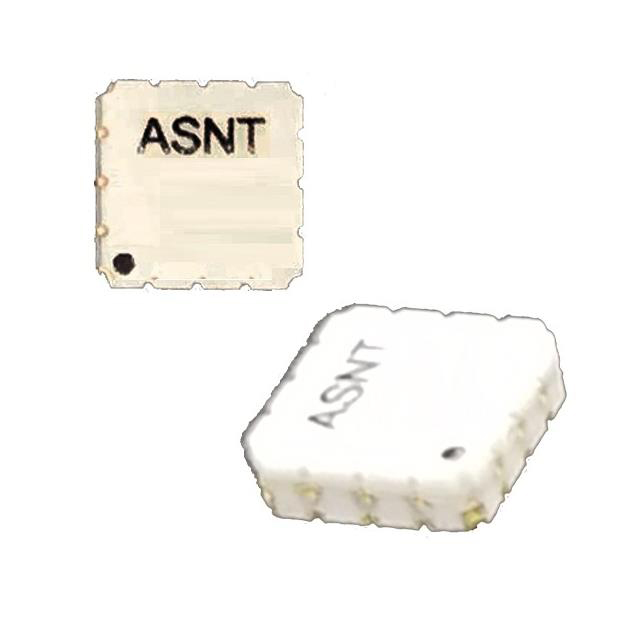
- Part No.:
- ASNT8143-KHC
- Manufacturer:
- ADSANTEC
- Category:
- Specialized ICs
- Package:
- 24-CQFN Exposed Pad
- Description:
- IC PSEUDORANDOM BIN SEQ 24CQFN
- Quantity:
Unit Price:$0
Ext Price:$0
- Payment:

- Shipping:


Product Details
ASNT8143-KHC - 24 Gb/s Selectable PRBS Generator
ADSANTEC ASNT8143-KHC is a SiGe pseudo-random binary sequence generator with selectable PRBS9 or PRBS10 operation, differential CML interfaces and a custom 24-pin CQFN package with a center heat slug. The LCDChip package record is 24-CQFN Exposed Pad.
Confirm the exact ordering code, package drawing and supply configuration against the manufacturer documentation before board release.
Overview
ASNT8143-KHC generates a 511-bit or 1023-bit PRBS using selectable ninth- or tenth-order polynomials. A differential asynchronous active-low reset prevents a locked all-zero sequence state. The device provides a main differential data output and a second sequence output delayed by half a period. The manufacturer specifies clock/data operation from DC to 24 Gb/s under its stated conditions.
Key Advantages
Control the PRBS9 or PRBS10 sequence using the off10 input.
Differential CML data is specified for operation to 24 Gb/s.
A half-period-delayed copy supports manufacturer-described external MUX or XOR test arrangements.
Asynchronous differential preset drives the sequence register out of the forbidden all-zero state.
Feature Summary
PRBS9: 2^9 - 1 bits; PRBS10: 2^10 - 1 bits.
Differential CML clock, reset and two data-output pairs.
Single +3.3 V or -3.3 V configuration, with configuration-dependent termination.
Manufacturer custom 24-pin CQFN with a backside center heat slug.
Package & Footprint
The original LCDChip record says 24-CQFN Exposed Pad. Its package registry contains the same normalized name and maps it to /upload/package/24-CQFN-Exposed-Pad.jpg. The ADSANTEC data sheet calls the device a custom 24-pin CQFN with a center heat slug; use its package drawing and pin-number table for the actual footprint. The generic package label alone does not establish mechanical interchangeability.

- Match pin-1 orientation and the ADSANTEC 24-pin drawing.
- Connect the center heat slug as directed for the selected supply configuration.
- Design differential CML traces and terminations for the intended data rate.
The registered JPG is missing locally and returns HTTP 404 on the production site. The manufacturer drawing, not this unavailable generic image, governs the footprint.
Pin Functions
The manufacturer's terminal-functions table identifies these exact signals and package pins:
Differential high-speed CML clock input.
Differential asynchronous active-low reset input.
Main differential PRBS data output.
Half-period-delayed differential sequence output.
CMOS polynomial-selection input; check the manufacturer's control truth table.
VCC: even pins 2-24. VEE: pins 1, 13 and 19.
Use the ADSANTEC drawing for orientation. Its electrical table contains a control-signal naming inconsistency; verify OFF10 control levels directly before implementation.
Key Specifications
| Device function | Selectable PRBS9 / PRBS10 generator |
|---|---|
| PRBS9 length | 511 bits, polynomial x^9 + x^4 + 1 |
| PRBS10 length | 1023 bits, polynomial x^10 + x^7 + 1 |
| Output data rate | DC to 24 Gb/s, manufacturer-specified |
| Clock input frequency | DC to 24 GHz, electrical-characteristics table |
| Supply arrangement | +3.3 V or -3.3 V single supply; configuration-dependent I/O termination |
| Negative-supply test condition | VCC = 0 V; VEE = -3.3 V nominal |
| Power consumption | 805 mW, manufacturer typical specification |
| Output swing | 280-440 mV single-ended, specified CML data output |
| Output jitter | 2.5 ps peak-to-peak, manufacturer table |
| Package | Custom 24-pin CQFN with center heat slug |
Electrical figures are from ADSANTEC Rev. 1.0.3 under its stated test configuration; absolute-maximum values are not operating targets.
Replacement Considerations
No pin-compatible substitute is established by the manufacturer's document. Compare any proposed generator for exact PRBS polynomials and lengths, differential CML electrical levels, reset behavior, clock/data rate, supply arrangement, 24-pin footprint and thermal-pad connection. The ASNT5150 and ASNT5140 are shown in the manufacturer's external frequency-doubling examples as a MUX and XOR device; they are not replacements for ASNT8143-KHC. No unverified LCDChip alternative link is asserted.
Manufacturer Information
ADSANTEC (Advanced Science And Novel Technology Company) publishes the ASNT8143-KHC Rev. 1.0.3 data sheet with functional description, terminal functions, electrical characteristics and the custom CQFN package drawing. Verify the current controlled revision and exact marking before design or procurement decisions.
Applications
Generate repeatable PRBS9 or PRBS10 patterns for signal-chain evaluation.
Exercise a suitable differential high-speed receiver with controlled patterns.
Use the main and delayed outputs in a manufacturer-described test arrangement.
Measure link behavior over an application-specific rate and termination configuration.
Quality & Authenticity
Check the ASNT8143-KHC marking, traceability, 24-pin CQFN geometry and heat-slug design against ADSANTEC documentation. Qualify the chosen supply and termination scheme on the actual PCB; a generic package image is insufficient for authenticity or footprint approval.
FAQ
Which sequences can ASNT8143-KHC generate?
Its selectable PRBS9 and PRBS10 modes produce 511-bit and 1023-bit sequences, respectively.
What are the two output pairs?
QP/QN carries the main sequence; QXORP/QXORN carries a copy delayed by half a sequence period.
Can it use a positive supply?
Yes, ADSANTEC describes +3.3 V and -3.3 V configurations, with different PCB and termination needs.
Is the package image available?
No. The registered site JPG currently returns HTTP 404 and must be supplied and visually checked before publication.
Engineering Notice
Review the ADSANTEC terminal table, package drawing, CML termination, reset and supply-configuration instructions for the actual design. Resolve the data-sheet OFF10 naming inconsistency with the manufacturer if precise control thresholds are required. The production package JPG is unavailable; do not publish this draft until the image, footprint and page presentation have been checked.
ASNT8143-KHC Information
- Specifications
- Tags
- Product attributes
- Attribute value
- Manufacturer:
- ADSANTEC
- Series:
- -
- Package/Case:
- 24-CQFN Exposed Pad
- Packaging:
- Retail Package
- Product Status:
- Active
- Programmable:
- Not Verified
- Type:
- Pseudorandom Binary Sequence Generator
- Applications:
- -
- Mounting Type:
- Surface Mount
- Supplier Device Package:
- 24-CQFN (4x4)
- Grade:
- -
- Qualification:
- -
- Include Parts
- Popular Search
The following parts include "ASNT8143-KHC" in Silicon Labs ASNT8143-KHC.
- Part Number
- Manufacturer
- Package
- Description
- CAP200DG-TL Power Integrations 8-SOIC (0.154", 3.90mm Width) IC AUTOMATIC DISCHARGE 8SO
- ATSHA204A-MAHDA-T Microchip Technology 8-UFDFN Exposed Pad IC AUTHENTICATION CHIP 8UDFN
- ATSHA204A-SSHDA-T Microchip Technology 8-SOIC (0.154", 3.90mm Width) IC AUTHENTICATION CHIP 8SOIC
- ATSHA204A-STUCZ-T Microchip Technology TO-236-3, SC-59, SOT-23-3 IC AUTHENTICATION CHIP SOT23-3
- ATECC608B-MAHDA-T Microchip Technology 8-UFDFN Exposed Pad IC AUTHENTICATION CHIP 8UDFN
- ATECC608B-MAHCZ-S Microchip Technology 8-UFDFN Exposed Pad IC AUTHENTICATION CHIP 8UDFN
- ATECC608B-SSHDA-T Microchip Technology 8-SOIC (0.154", 3.90mm Width) IC AUTHENTICATION CHIP 8SOIC
- ATECC608B-MAHDA-S Microchip Technology 8-UFDFN Exposed Pad IC AUTHENTICATION CHIP 8UDFN
- ATECC608A-MAHDA-S Microchip Technology 8-UFDFN Exposed Pad IC AUTHENTICATION CHIP 8UDFN
- ATECC608B-MAVDA-T Microchip Technology 8-UFDFN Exposed Pad IC AUTHENTICATION CHIP 8UDFN
The following parts are popular search parts in Test and Measurement.
Inventory:1,114
Please send an inquiry. Send us your inquiry, and we will respond immediately.


