 Hello! now
 tms@lcdchip.com



Alpha & Omega Semiconductor Inc. AOZ32034AQV
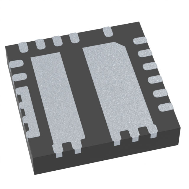
- Part No.:
- AOZ32034AQV
- Manufacturer:
- Alpha & Omega Semiconductor Inc.
- Category:
- Specialized ICs
- Package:
- 23-PowerTFQFN
- Description:
- IC COIL DRIVER 23QFNB
- Quantity:
Unit Price:$0
Ext Price:$0
- Payment:

- Shipping:


Product Details
AOZ32034AQV - Half-Bridge Coil Driver for Wireless Charging
Alpha & Omega Semiconductor AOZ32034AQV integrates high-side and low-side N-channel MOSFETs with a half-bridge driver and adjustable slew-rate control. The exact device is supplied in a thermally enhanced 23-pin, 4 × 4 mm QFN package, represented in the LCDChip catalog as 23-PowerTFQFN.
Designed for wireless-charger transmitter power stages; verify coil, resonant tank, thermal design, and gate-drive timing in the complete system.
Overview
AOZ32034AQV is an integrated half-bridge power stage intended for wireless-charger transmitter coil drive. It combines N-channel power MOSFETs, a high/low-side driver, an integrated bootstrap diode, and a slew-rate control input. Designers can pair half-bridge stages in a full-bridge arrangement for a resonant transmitter, subject to the manufacturer's application circuit and thermal limits.
Key Advantages
Integrated power stage
High-side and low-side MOSFETs and their driver are contained in one compact package.
Controllable edge rate
The SRC connection adjusts drive behavior to balance switching losses and electromagnetic interference.
Bootstrap integration
An integrated bootstrap diode simplifies the high-side supply circuit, with an external capacitor still required.
Protection functions
The datasheet identifies VCC undervoltage lockout and overtemperature protection.
Feature Summary
Wireless-power drive
The manufacturer positions the device as a 15–50 W coil-driver solution, contingent on complete system design.
Wide VIN range
Recommended VIN operation is 3.8–28 V, covering common 12 V and 24 V power rails.
Low MOSFET resistance
Both integrated MOSFET paths have 7.5 mΩ typical on-resistance under the datasheet's stated test conditions.
Compact thermal package
The manufacturer's package is a thermally enhanced 23-pin 4 × 4 mm QFN.
Package & Footprint
The official AOZ32034AQV datasheet specifies a 23-pin 4 × 4 mm thermally enhanced QFN. The manufacturer's package page identifies QFN4x4B-23L / QFN4x4B_23L_EP2_S. LCDChip's existing normalized package is 23-PowerTFQFN. Confirm the exact land pattern and exposed-pad arrangement from the manufacturer drawing before board release; the normalized catalog label is not a mechanical specification.

- Use the manufacturer's QFN4x4B-23L package drawing for pad and thermal geometry.
- Connect all repeated VIN, VHB, and PGND pads as specified.
- Keep the VCC bypass capacitor close to VCC and AGND.
The registered package JPG is awaiting upload on the production site.
Pin Functions
Selected assignments from the manufacturer's 23-pin pin-description table:
Adjusts internal driver slew rate.
High-side and low-side PWM inputs.
Power input; connect all VIN pads together.
Half-bridge switching node; connect all VHB pads together.
Power-ground connections.
Bootstrap capacitor connection; capacitor goes to VHB.
Analog supply and analog ground.
No-connect pins; manufacturer note requires them to float.
Use the complete manufacturer pin diagram and recommended layout when placing the package.
Key Specifications
| Device type | Integrated half-bridge MOSFET power stage and driver |
|---|---|
| Primary application | Wireless-charger transmitter coil drive |
| Recommended VIN | 3.8 to 28 V |
| Recommended VCC | 4.75 to 5.5 V |
| Ambient temperature | -40 to +125 °C |
| High-side MOSFET RDS(on) | 7.5 mΩ typical at VIN 12 V, VCC 5 V, bootstrap-to-switch voltage 5 V and switch current 1 A |
| Low-side MOSFET RDS(on) | 7.5 mΩ typical at VIN 12 V, VCC 5 V and switch current 1 A |
| Integrated protection | VCC undervoltage lockout and overtemperature protection |
| Bootstrap | Integrated diode; external capacitor between BST and VHB |
| Package | Thermally enhanced 23-pin 4 × 4 mm QFN |
| Output-power positioning | 15 to 50 W wireless-transmitter coil driver; system-dependent |
Typical electrical values apply only at their stated test conditions. Do not treat absolute-maximum stress limits as recommended operation.
Replacement Considerations
No pin-compatible replacement is established here. Compare any proposed alternative against the exact 23-pin package drawing, integrated MOSFET resistance, power and control supplies, HIN/LIN logic and timing, slew-rate control, thermal design, and bootstrap connection. A related half-bridge device is not a drop-in substitute based solely on function or package size. No LCDChip internal replacement link is included without an exact API-confirmed product and manufacturer-supported relationship.
Manufacturer Information
AOZ32034AQV is specified by Alpha & Omega Semiconductor. The manufacturer's AOZ32034AQV datasheet and QFN4x4B-23L package drawing control electrical and mechanical design decisions.
Applications
Wireless charging transmitters
Drive a transmitter coil through a properly designed resonant power stage.
Full-bridge stages
Pair two half-bridges when the complete design requires a full-bridge topology.
Compact power conversion
Use the integrated MOSFET/driver stage where footprint and switching behavior meet system requirements.
EMI-sensitive designs
Adjust slew-rate control as part of an evaluated loss, thermal, and EMI tradeoff.
Quality & Authenticity
Verify the complete order code and traceability for received material. Inspect package marking against the manufacturer's marking documentation and confirm handling and reflow requirements through the approved quality process. This description does not imply a test result or authorized-distribution claim.
FAQ
Are the high- and low-side MOSFETs integrated?
Yes. AOZ32034AQV integrates both N-channel MOSFETs and their half-bridge driver.
Can the 28 V VIN limit be used as a VCC supply?
No. The manufacturer recommends VIN from 3.8 to 28 V and separately recommends VCC from 4.75 to 5.5 V.
Does it need an external bootstrap capacitor?
Yes. The diode is integrated, while the datasheet directs an external capacitor between BST and VHB.
Engineering Notice
Validate electrical operating conditions, switching timing, thermal dissipation, EMI, and the exact QFN land pattern against the latest manufacturer documents. The catalog package image is not yet available online. This page does not state real-time inventory or pricing.
AOZ32034AQV Information
- Specifications
- Tags
- Product attributes
- Attribute value
- Manufacturer:
- Alpha & Omega Semiconductor Inc.
- Series:
- -
- Package/Case:
- 23-PowerTFQFN
- Packaging:
- Tape & Reel (TR)
- Product Status:
- Active
- Programmable:
- Not Verified
- Type:
- Coil Driver
- Applications:
- -
- Mounting Type:
- Surface Mount
- Supplier Device Package:
- 23-QFNB (4x4)
- Grade:
- -
- Qualification:
- -
- Include Parts
- Popular Search
The following parts include "AOZ32034AQV" in Silicon Labs AOZ32034AQV.
- Part Number
- Manufacturer
- Package
- Description
- CAP200DG-TL Power Integrations 8-SOIC (0.154", 3.90mm Width) IC AUTOMATIC DISCHARGE 8SO
- ATSHA204A-MAHDA-T Microchip Technology 8-UFDFN Exposed Pad IC AUTHENTICATION CHIP 8UDFN
- ATSHA204A-SSHDA-T Microchip Technology 8-SOIC (0.154", 3.90mm Width) IC AUTHENTICATION CHIP 8SOIC
- ATSHA204A-STUCZ-T Microchip Technology TO-236-3, SC-59, SOT-23-3 IC AUTHENTICATION CHIP SOT23-3
- ATECC608B-MAHDA-T Microchip Technology 8-UFDFN Exposed Pad IC AUTHENTICATION CHIP 8UDFN
- ATECC608B-MAHCZ-S Microchip Technology 8-UFDFN Exposed Pad IC AUTHENTICATION CHIP 8UDFN
- ATECC608B-SSHDA-T Microchip Technology 8-SOIC (0.154", 3.90mm Width) IC AUTHENTICATION CHIP 8SOIC
- ATECC608B-MAHDA-S Microchip Technology 8-UFDFN Exposed Pad IC AUTHENTICATION CHIP 8UDFN
- ATECC608A-MAHDA-S Microchip Technology 8-UFDFN Exposed Pad IC AUTHENTICATION CHIP 8UDFN
- ATECC608B-MAVDA-T Microchip Technology 8-UFDFN Exposed Pad IC AUTHENTICATION CHIP 8UDFN
The following parts are popular search parts in Test and Measurement.
Inventory:4,080
Please send an inquiry. Send us your inquiry, and we will respond immediately.


