 Hello! now
 tms@lcdchip.com



Analog Devices Inc. AD9942BBCZ
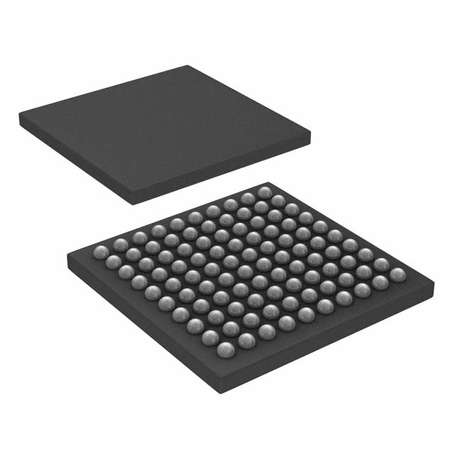
- Part No.:
- AD9942BBCZ
- Manufacturer:
- Analog Devices Inc.
- Category:
- Specialized ICs
- Package:
- 100-LFBGA, CSPBGA
- Description:
- IC CCD SGNL PROC 14BIT 100CSPBGA
- Quantity:
Unit Price:$0
Ext Price:$0
- Payment:

- Shipping:


Product Details
AD9942BBCZ - Dual-Channel 14-Bit CCD Signal Processor
The Analog Devices AD9942BBCZ integrates two CCD analog front ends and a programmable Precision Timing core. It is supplied in a 100-ball 9 x 9 mm CSP_BGA package and is obsolete.
Overview
Each channel supports CCD signal conditioning at pixel rates up to 40 MHz. The device combines correlated double sampling, variable gain, optical-black clamping and 14-bit conversion with clock and reset-gate timing drivers. It was designed for dual-output imaging architectures, not as a standalone image sensor.
Key Benefits
- Two matched imaging channels in one device.
- 14-bit conversion at up to 40 MSPS per channel.
- Integrated CCD clock and reset-gate drivers.
- Fine programmable timing adjustment below 550 ps resolution.
- Compact 9 x 9 mm 100-ball package.
Functional Features
Each analog front end includes a correlated double sampler, 0 to 18 dB 9-bit VGA, optical-black clamp and ADC. The timing core drives RG_A/RG_B and H1A to H4A/H1B to H4B clock sets, including a four-phase H-clock mode. A six-wire serial interface programs both channels.
Package & Footprint
Analog Devices lists the exact AD9942BBCZ order code in a 100-ball CSP_BGA, 9 x 9 x 1.4 mm. The catalog describes a 100-LFBGA/CSPBGA. The local package register has a generic 100-LFBGA entry but does not by itself establish the 9 x 9 mm ball map; check the manufacturer's controlled footprint. Its registered JPG is absent.

- Confirm 9 x 9 mm body and ball grid.
- Use the official ball map for routing.
- Validate moisture handling and reflow profile.
Ball Functions
Channel A uses CCDIN_A at A1, serial controls SL_A at B2, SDATA_A at C2 and SCK_A at D2, and reference balls REFT_A at C1 and REFB_A at D1. Channel B has corresponding CCDIN_B, serial and reference connections. H1 through H4 and RG outputs drive the CCD timing path. Follow the manufacturer's full 100-ball assignment for supplies, grounds, drivers and no-connects.
Key Specifications
| Function | Dual-channel CCD signal processor |
|---|---|
| Exact order code | AD9942BBCZ |
| ADC resolution | 14 bits per channel |
| Maximum pixel rate | 40 MHz per channel |
| ADC rate | 40 MSPS |
| VGA range | 0 to 18 dB, 9-bit control |
| Timing resolution | Less than 550 ps |
| Serial interface | Six-wire programmable |
| Clock driver | 3 V horizontal and reset-gate outputs |
| Temperature range | -25 to +85 degrees C |
| Package | 100-ball CSP_BGA, 9 x 9 x 1.4 mm |
| Lifecycle | Obsolete |
Check the full manufacturer timing and electrical tables for limits and loading.
Replacement Considerations
Analog Devices' discontinuance notice names ADDI7013BBCZ as a replacement candidate but explicitly says it is not pin-to-pin compatible. No database-verified drop-in alternative is linked. Redesign and verify timing, register configuration, clock drivers, power domains and the ball map before substitution.
Manufacturer Information
Analog Devices publishes the AD9942 Rev. A data sheet and lists AD9942BBCZ as obsolete. Its product discontinuance notice identifies the non-pin-compatible replacement candidate. Use current manufacturer documents and equipment-specific requirements for repair decisions.
Applications
- Dual-channel CCD imaging systems.
- Legacy digital still and video cameras.
- High-speed imaging equipment designed for the AD9942 ball map.
Quality & Authenticity
For this obsolete device, verify full markings, lot traceability, storage history, solder-ball condition and package dimensions. Public broker inventory is not a confirmed authorized live quotation. The catalog price and quantity remain unverified and must not be represented as current distributor terms.
FAQ
How many imaging channels are available?
Two, each supporting up to 40 MHz pixel rates.
Does it include CCD timing outputs?
Yes, horizontal and reset-gate drivers are integrated.
Is the suggested replacement pin-compatible?
No. Analog Devices marks ADDI7013BBCZ as not pin-to-pin compatible.
Is the package image verified?
No. The local 100-LFBGA JPG is absent and the exact ball-map match requires review.
Engineering Notice
Validate the CCD input network, clamp levels, ADC timing, serial control, supply sequencing and every ball assignment before board use. Missing package JPG, unresolved registry footprint details and unverified live authorized inventory and tier prices prohibit publication.
AD9942BBCZ Information
- Specifications
- Tags
- Product attributes
- Attribute value
- Manufacturer:
- Analog Devices Inc.
- Series:
- -
- Package/Case:
- 100-LFBGA, CSPBGA
- Packaging:
- Tray
- Product Status:
- Obsolete
- Programmable:
- Not Verified
- Type:
- CCD Signal Processor, 14-Bit
- Applications:
- Digital Camera
- Mounting Type:
- Surface Mount
- Supplier Device Package:
- 100-CSPBGA (9x9)
- Grade:
- -
- Qualification:
- -
- Include Parts
- Popular Search
The following parts include "AD9942BBCZ" in Silicon Labs AD9942BBCZ.
- Part Number
- Manufacturer
- Package
- Description
- CAP200DG-TL Power Integrations 8-SOIC (0.154", 3.90mm Width) IC AUTOMATIC DISCHARGE 8SO
- ATSHA204A-MAHDA-T Microchip Technology 8-UFDFN Exposed Pad IC AUTHENTICATION CHIP 8UDFN
- ATSHA204A-SSHDA-T Microchip Technology 8-SOIC (0.154", 3.90mm Width) IC AUTHENTICATION CHIP 8SOIC
- ATSHA204A-STUCZ-T Microchip Technology TO-236-3, SC-59, SOT-23-3 IC AUTHENTICATION CHIP SOT23-3
- ATECC608B-MAHDA-T Microchip Technology 8-UFDFN Exposed Pad IC AUTHENTICATION CHIP 8UDFN
- ATECC608B-MAHCZ-S Microchip Technology 8-UFDFN Exposed Pad IC AUTHENTICATION CHIP 8UDFN
- ATECC608B-SSHDA-T Microchip Technology 8-SOIC (0.154", 3.90mm Width) IC AUTHENTICATION CHIP 8SOIC
- ATECC608B-MAHDA-S Microchip Technology 8-UFDFN Exposed Pad IC AUTHENTICATION CHIP 8UDFN
- ATECC608A-MAHDA-S Microchip Technology 8-UFDFN Exposed Pad IC AUTHENTICATION CHIP 8UDFN
- ATECC608B-MAVDA-T Microchip Technology 8-UFDFN Exposed Pad IC AUTHENTICATION CHIP 8UDFN
The following parts are popular search parts in Test and Measurement.
Inventory:1,624
Please send an inquiry. Send us your inquiry, and we will respond immediately.


