 Hello! now
 tms@lcdchip.com



Analog Devices Inc. AD9867BCPZ

- Part No.:
- AD9867BCPZ
- Manufacturer:
- Analog Devices Inc.
- Category:
- Specialized ICs
- Package:
- 64-VFQFN Exposed Pad, CSP
- Description:
- IC BROADBAND FRONT-END 64LFCSP
- Quantity:
Unit Price:$0
Ext Price:$0
- Payment:

- Shipping:


Product Details
AD9867BCPZ — Broadband Modem Mixed-Signal Front End
AD9867BCPZ from Analog Devices combines a 10-bit transmit DAC, a 10-bit receive ADC, receive programmable-gain amplification, filtering, flexible digital interfaces and clock generation for broadband-modem transceivers. The exact orderable model uses a 64-lead, 9 mm × 9 mm LFCSP with exposed pad.
Analog Devices lists AD9867BCPZ as production but marks the AD9867 family not recommended for new designs. Review lifecycle and application fit before design-in.
Overview
The AD9867 is a broadband-modem mixed-signal front end with transmit and receive signal paths on one 3.3 V CMOS device. Its transmit path has a bypassable 2×/4× interpolation filter and a 10-bit current-output DAC. Its receive path has a selectable input, programmable-gain amplifier, tunable low-pass filter and 10-bit ADC. The digital datapath can support half-duplex or full-duplex operation, with an SPI-compatible control port for configuration.
Key Advantages
Integrated transmit path
10-bit DAC with selectable interpolation and up to 250 MSPS DAC update rate.
Integrated receive path
10-bit ADC up to 75 MSPS with a low-noise programmable-gain amplifier.
Flexible duplex operation
Digital datapath and power modes accommodate half-duplex and full-duplex architectures.
Clock consolidation
On-chip PLL and clock distribution derive internal clocks and two auxiliary outputs from one clock source.
Feature Summary
Tx conditioning
2×/4× interpolation filtering and digital transmit-power control over a 7.5 dB range in 0.5 dB steps.
Rx conditioning
Dual-channel multiplexed input, optional 6 dB overload attenuation and gain adjustment from −12 dB to +48 dB without the attenuator.
Programmable filtering
Receive low-pass cutoff can be adjusted over approximately 22 MHz to 38 MHz or bypassed.
Power management
Individual functional blocks can use reduced-power or power-down modes as required by the duplex plan.
Package & Footprint
Analog Devices identifies the exact AD9867BCPZ orderable model as a 64-lead LFCSP, 9 mm × 9 mm × 0.75 mm, with exposed pad. LCDChip records its package as 64-VFQFN Exposed Pad, CSP; the existing package register has 64-VFQFN Exposed Pad. These names require footprint and outline comparison before asserting mechanical equivalence. Follow the manufacturer's package drawing and exposed-pad guidance.
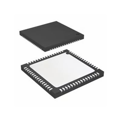
- Confirm 64-lead 9 mm × 9 mm LFCSP dimensions and pin-1 orientation.
- Use the manufacturer-recommended land pattern and exposed-pad connection.
- Separate sensitive analog routing from the fast digital and clock paths.
The expected package JPG is absent locally and returns HTTP 404 on the production site. This catalog image is not a verified footprint drawing.
Pin Functions
Signal groups below follow the manufacturer's functional diagram. Use the official pin-configuration drawing for exact pin numbers and wiring.
Differential current outputs from the transmit DAC.
Selectable differential receive-channel inputs.
Shared and mode-dependent digital datapath signals.
Transmit and receive sample clocks and synchronization control.
Clock-source connections and auxiliary clock outputs.
SPI-compatible programming, power-down and supply connections; see full pin table.
Key Specifications
| Exact orderable model | AD9867BCPZ |
|---|---|
| Function | Broadband-modem mixed-signal front end |
| Technology | 3.3 V CMOS |
| Transmit converter | 10-bit DAC, up to 250 MSPS update rate |
| Transmit interpolation | Bypassable 2× or 4× filter |
| Receive converter | 10-bit ADC, 5 MSPS to 75 MSPS operating span |
| RxPGA gain | −12 dB to +48 dB without optional attenuation |
| Optional input attenuation | 6 dB, with external-network-dependent extensions |
| Receive LPF | Adjustable cutoff over about 22 MHz to 38 MHz, or bypass |
| Duplex operation | Half-duplex or full-duplex |
| Operating temperature | −40 °C to +85 °C |
| Manufacturer package | 64-lead LFCSP, 9 mm × 9 mm × 0.75 mm, exposed pad |
| Manufacturer lifecycle | Exact part: production; family: not recommended for new designs |
Sample-rate and gain limits depend on the complete operating conditions. Consult the current full datasheet and hardware design guidance.
Replacement Considerations
A replacement must match the converter resolution and rates, receive gain and filtering, clocking, digital timing, supply domains, 64-lead package outline and exposed-pad layout. The manufacturer's family lifecycle note makes a new-design alternative review important. No family member is represented here as a drop-in replacement.
No internal alternative-product link is asserted without an exact LCDChip catalog match and engineering review.
Manufacturer Information
Analog Devices identifies AD9867BCPZ as a production part within the AD9867 mixed-signal front-end family. Its product page labels the family not recommended for new designs. Functional parameters are taken from the official AD9867 data sheet, revision SpB, and the exact-model package entry on the manufacturer product page.
Applications
Power-line networking
The application explicitly identified by Analog Devices for this broadband-modem front end.
Legacy broadband modems
Transmit and receive front-end support where the existing interface is already validated.
Duplex transceivers
Integrated converter and filtering paths for systems that match the device's timing requirements.
Hardware maintenance
Exact-part service in equipment with a confirmed 64-lead package and board footprint.
Quality & Authenticity
Verify the AD9867BCPZ orderable suffix, marking, traceability and 64-lead package against current Analog Devices documentation. Distinguish the manufacturer's LFCSP outline from the catalog's QFN/CSP wording. The missing catalog JPG cannot substantiate supplied-device identity or footprint compatibility.
FAQ
Does AD9867BCPZ integrate both Tx and Rx converters?
Yes. It includes a 10-bit transmit DAC and a 10-bit receive ADC.
What is the maximum ADC sample rate?
The manufacturer specifies operation up to 75 MSPS under its stated conditions.
Is this part recommended for a new design?
Analog Devices marks the AD9867 family not recommended for new designs, although the exact model is listed as production.
Can the catalog package name be used directly for PCB layout?
No. Check the exact 64-lead LFCSP drawing, pin-1 orientation and exposed-pad land pattern.
Engineering Notice
Verify transmit-output loading, receive analog levels, digital timing, PLL and clock-source design, decoupling, power sequencing and exposed-pad thermal connection in the full system. Reconcile the catalog package naming and restore the missing production JPG before publication.
AD9867BCPZ Information
- Specifications
- Tags
- Product attributes
- Attribute value
- Manufacturer:
- Analog Devices Inc.
- Series:
- MxFE™
- Package/Case:
- 64-VFQFN Exposed Pad, CSP
- Packaging:
- Bulk
- Product Status:
- Active
- Programmable:
- Not Verified
- Type:
- Broadband Front-End
- Applications:
- Power Line Networking
- Mounting Type:
- Surface Mount
- Supplier Device Package:
- 64-LFCSP-VQ (9x9)
- Grade:
- -
- Qualification:
- -
- Include Parts
- Popular Search
The following parts include "AD9867BCPZ" in Silicon Labs AD9867BCPZ.
- Part Number
- Manufacturer
- Package
- Description
- CAP200DG-TL Power Integrations 8-SOIC (0.154", 3.90mm Width) IC AUTOMATIC DISCHARGE 8SO
- ATSHA204A-MAHDA-T Microchip Technology 8-UFDFN Exposed Pad IC AUTHENTICATION CHIP 8UDFN
- ATSHA204A-SSHDA-T Microchip Technology 8-SOIC (0.154", 3.90mm Width) IC AUTHENTICATION CHIP 8SOIC
- ATSHA204A-STUCZ-T Microchip Technology TO-236-3, SC-59, SOT-23-3 IC AUTHENTICATION CHIP SOT23-3
- ATECC608B-MAHDA-T Microchip Technology 8-UFDFN Exposed Pad IC AUTHENTICATION CHIP 8UDFN
- ATECC608B-MAHCZ-S Microchip Technology 8-UFDFN Exposed Pad IC AUTHENTICATION CHIP 8UDFN
- ATECC608B-SSHDA-T Microchip Technology 8-SOIC (0.154", 3.90mm Width) IC AUTHENTICATION CHIP 8SOIC
- ATECC608B-MAHDA-S Microchip Technology 8-UFDFN Exposed Pad IC AUTHENTICATION CHIP 8UDFN
- ATECC608A-MAHDA-S Microchip Technology 8-UFDFN Exposed Pad IC AUTHENTICATION CHIP 8UDFN
- ATECC608B-MAVDA-T Microchip Technology 8-UFDFN Exposed Pad IC AUTHENTICATION CHIP 8UDFN
The following parts are popular search parts in Test and Measurement.
Inventory:2,928
Please send an inquiry. Send us your inquiry, and we will respond immediately.


