 Hello! now
 tms@lcdchip.com



Analog Devices Inc. AD8190ACPZ
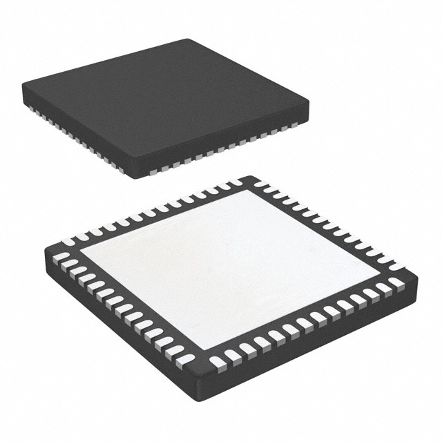
- Part No.:
- AD8190ACPZ
- Manufacturer:
- Analog Devices Inc.
- Category:
- Specialized ICs
- Package:
- 56-VFQFN Exposed Pad, CSP
- Description:
- IC HDMI/DVI SWITCH 56LFCSP
- Quantity:
Unit Price:$0
Ext Price:$0
- Payment:

- Shipping:


Product Details
AD8190ACPZ - 2:1 HDMI/DVI Switch with Equalization
Analog Devices AD8190ACPZ selects one of two HDMI/DVI source links for a single receiver, with equalized TMDS inputs and pre-emphasized outputs, in the manufacturer's 56-lead 8 mm by 8 mm LFCSP exposed-pad package.
ADI explicitly lists this order code and package. The catalog's VFQFN/CSP package terminology requires mechanical reconciliation before publication.
Overview
The AD8190 is a two-input, one-output HDMI/DVI link switch. Four differential high-speed TMDS channels per link carry the video signals, while four auxiliary low-speed channels route DDC and other control lines. Input equalization and output pre-emphasis support longer cable paths in display and video-routing equipment.
Key Advantages
Switches four TMDS pairs together with four auxiliary signals per input.
Equalized inputs and pre-emphasized outputs address cable and board losses.
The manufacturer specifies data rates from 250 Mbps to 1.65 Gbps under its operating conditions.
Output-disable and switch settings permit reduced-power arrangements.
Feature Summary
Three data pairs and a pixel-clock pair are routed for each video link.
Four bidirectional low-speed signals can route DDC and additional controls.
On-chip 50-ohm terminations are globally selectable as documented by ADI.
An I2C slave port sets channel selection, termination and equalization modes.
Package & Footprint
ADI lists AD8190ACPZ as a 56-lead, 8 mm by 8 mm LFCSP with exposed pad. The original product database calls the package 56-VFQFN Exposed Pad, CSP; the local package registry includes 56-VFQFN Exposed Pad. Similar broad package labels are not proof that the registered image or land pattern matches the controlled ADI LFCSP drawing. Reconcile the manufacturer's outline and exposed-pad dimensions before use.

- Compare the 8 mm by 8 mm LFCSP body with the registered outline.
- Check pin-one orientation and all 56 contact positions.
- Confirm exposed-pad land, grounding and thermal guidance.
The registered package JPG is unavailable locally and returns 404 on the production site; its content has not been verified.
Pin Functions
ADI's functional diagram and pin descriptions identify these groups:
Use the manufacturer's 56-lead pin map for exact pin numbers, supply partitioning and exposed-pad handling.
Key Specifications
| Exact order code | AD8190ACPZ |
|---|---|
| Manufacturer | Analog Devices Inc. |
| Function | 2:1 HDMI/DVI switch with equalization |
| High-speed channels | Four TMDS differential pairs per source |
| Auxiliary channels | Four bidirectional lines per source |
| TMDS data rate | 250 Mbps to 1.65 Gbps, manufacturer conditions |
| Pixel clock range | 25 MHz to 165 MHz, manufacturer conditions |
| High-speed supply class | 3.3 V single-supply operation as described by ADI |
| Auxiliary voltage support | 3.3 V to 5 V flexible auxiliary operation |
| Configuration port | I2C slave interface |
| Operating temperature | -40 to +85 degrees Celsius |
| Manufacturer package | 56-lead, 8 mm by 8 mm LFCSP with exposed pad |
Signal-integrity and cable-length statements depend on cable, board layout, supply and equalization settings; use the datasheet test conditions.
Replacement Considerations
Match the 56-lead LFCSP footprint, exposed pad, TMDS channel topology, auxiliary/DDC voltage behavior, I2C register configuration, equalization, output termination and timing. A related HDMI switch is not automatically a drop-in replacement. No internal alternative is linked because an exact product and package match has not been verified by the catalog API.
Manufacturer Information
The catalog names Analog Devices Inc. ADI's product-selection table explicitly lists AD8190ACPZ in the 56-lead 8 mm by 8 mm exposed-pad LFCSP, and the Rev. 0 datasheet documents the switch architecture and pin functions.
Applications
Selection between two HDMI/DVI video sources.
Source routing with cable equalization ahead of a receiver.
Video and DDC/control path switching.
Compact high-speed link selection on display boards.
Quality & Authenticity
Verify complete marking, LFCSP body, exposed pad and lot traceability. Inspect mounting and thermal connections, then qualify TMDS eye performance, DDC continuity and I2C control behavior in the actual board environment.
FAQ
What does the AD8190 switch?
One of two HDMI/DVI source links, including four TMDS pairs and four auxiliary signals, to a receiver.
How is source selection controlled?
An I2C slave interface configures high-speed and auxiliary switch modes.
Is the database VFQFN label equivalent to ADI LFCSP?
That equivalence has not been proven; compare the controlled ADI outline and board land pattern.
Is the package image verified?
No. The registered JPG is missing on the production site.
Engineering Notice
Before design or repair, verify the exact ACPZ order code, LFCSP package drawing versus the catalog VFQFN description, exposed-pad layout, TMDS signal integrity, DDC voltage limits, supplies and I2C configuration. The package mapping and production JPG are unresolved; this content must remain under review and must not be published.
AD8190ACPZ Information
- Specifications
- Tags
- Product attributes
- Attribute value
- Manufacturer:
- Analog Devices Inc.
- Series:
- -
- Package/Case:
- 56-VFQFN Exposed Pad, CSP
- Packaging:
- Tray
- Product Status:
- Active
- Programmable:
- Not Verified
- Type:
- HDMI/DVI Switch
- Applications:
- DVI, HDMI Signal Switching
- Mounting Type:
- Surface Mount
- Supplier Device Package:
- 56-LFCSP-VQ (8x8)
- Grade:
- -
- Qualification:
- -
- Include Parts
- Popular Search
The following parts include "AD8190ACPZ" in Silicon Labs AD8190ACPZ.
- Part Number
- Manufacturer
- Package
- Description
- CAP200DG-TL Power Integrations 8-SOIC (0.154", 3.90mm Width) IC AUTOMATIC DISCHARGE 8SO
- ATSHA204A-MAHDA-T Microchip Technology 8-UFDFN Exposed Pad IC AUTHENTICATION CHIP 8UDFN
- ATSHA204A-SSHDA-T Microchip Technology 8-SOIC (0.154", 3.90mm Width) IC AUTHENTICATION CHIP 8SOIC
- ATSHA204A-STUCZ-T Microchip Technology TO-236-3, SC-59, SOT-23-3 IC AUTHENTICATION CHIP SOT23-3
- ATECC608B-MAHDA-T Microchip Technology 8-UFDFN Exposed Pad IC AUTHENTICATION CHIP 8UDFN
- ATECC608B-MAHCZ-S Microchip Technology 8-UFDFN Exposed Pad IC AUTHENTICATION CHIP 8UDFN
- ATECC608B-SSHDA-T Microchip Technology 8-SOIC (0.154", 3.90mm Width) IC AUTHENTICATION CHIP 8SOIC
- ATECC608B-MAHDA-S Microchip Technology 8-UFDFN Exposed Pad IC AUTHENTICATION CHIP 8UDFN
- ATECC608A-MAHDA-S Microchip Technology 8-UFDFN Exposed Pad IC AUTHENTICATION CHIP 8UDFN
- ATECC608B-MAVDA-T Microchip Technology 8-UFDFN Exposed Pad IC AUTHENTICATION CHIP 8UDFN
The following parts are popular search parts in Test and Measurement.
Inventory:3,577
Please send an inquiry. Send us your inquiry, and we will respond immediately.


