 Hello! now
 tms@lcdchip.com



Analog Devices Inc. AD7341JP

- Part No.:
- AD7341JP
- Manufacturer:
- Analog Devices Inc.
- Category:
- Specialized ICs
- Package:
- 28-LCC (J-Lead)
- Description:
- IC DIGITALLY PROG FILTER 28PLCC
- Quantity:
Unit Price:$0
Ext Price:$0
- Payment:

- Shipping:


Product Details
AD7341JP — Voiceband Transmit Reconstruction Filter
AD7341JP is an Analog Devices transmit-path reconstruction filter for legacy voiceband modems. It combines a seventh-order switched-capacitor low-pass stage, a second-order continuous-time low-pass stage, programmable output attenuation and clock synchronization functions. The JP orderable variant is a 28-lead plastic leaded chip carrier (PLCC).
Analog Devices lists AD7341 as obsolete. This is a legacy-service part, not a recommended component for a new design.
Overview
The AD7341 filters the output of a separate voiceband DAC before the modem line interface. The manufacturer's historical data sheet pairs it with the AD7371 receive antialiasing filter, a separate ADC/DAC and a DSP in V.32/V.33-era modem architectures. The AD7341 itself is the transmit reconstruction filter; it does not contain the DAC, ADC, receive filter or complete modem.
Key Advantages
Dedicated Tx filtering
Switched-capacitor and continuous-time stages reconstruct the analog output of a separate DAC.
Digitally set attenuation
Programmable transmit-path attenuation spans 0 dB to −38 dB under the datasheet's conditions.
Clock coordination
Clock-divider and synchronization signals help align the filter with the converter update rate.
Defined legacy package
The manufacturer's ordering guide identifies JP as its 28-pin PLCC package option P-28A.
Feature Summary
Low-pass topology
Seventh-order switched-capacitor filter followed by a second-order continuous-time low-pass stage.
Voiceband response
The specification table gives a 3.5 kHz low-pass cutoff for the stated 288 kHz clock configuration.
Programmable clock division
Input-clock and synchronized-output divider controls support modem timing arrangements.
Parallel control
Data and write-control pins set attenuation and timing functions as described in the original data sheet.
Package & Footprint
The original Analog Devices ordering guide lists AD7341JP as a 28-pin plastic leaded chip carrier, package option P-28A. LCDChip records 28-LCC (J-Lead), and its package registry maps this to 28-LCC.jpg. The J-lead PLCC construction is consistent with the catalog's broad LCC wording, but the exact mechanical footprint must be checked against the manufacturer outline.
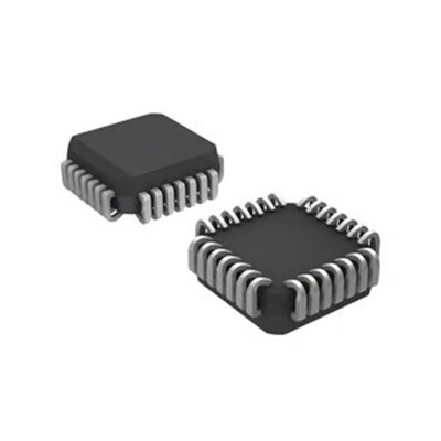
- Match package option P-28A and the manufacturer's top-view pin orientation.
- Check J-lead pad geometry before using an existing PLCC footprint.
- Verify board clearance and soldering requirements for repair work.
The expected catalog JPG is absent locally and returns HTTP 404 on the production site. Do not treat this missing image as a verified footprint drawing.
Pin Functions
The following groups follow the manufacturer's AD7341 pin diagram and specification table. Consult that diagram for exact numbered pins and the JP top view.
Analog transmit-path filter input and reconstructed output.
Filter clock input and converter synchronization connections.
Parallel attenuation-control data and write strobe.
Input clock-divider selection controls.
Synchronized output divider selection controls.
Analog and digital supply and ground connections; maintain the specified rails and decoupling.
Key Specifications
| Orderable model | AD7341JP |
|---|---|
| Manufacturer | Analog Devices |
| Function | Voiceband transmit reconstruction filter |
| Filter stages | Seventh-order switched-capacitor and second-order continuous-time low pass |
| Cutoff frequency | 3.5 kHz in the stated 288 kHz input-clock configuration |
| Programmable attenuation | 0 dB to −38 dB |
| Nominal positive rails | VDD and VCC approximately +5 V |
| Nominal negative rail | VSS approximately −5 V |
| Operating temperature | 0 °C to +70 °C for J versions |
| Manufacturer package | 28-pin PLCC, option P-28A |
| Catalog package | 28-LCC (J-Lead) |
| Lifecycle | Obsolete |
The scanned Rev. A specification table uses defined supply, clock, load and ambient conditions. Verify all timing and analog limits directly in the full original data sheet before circuit changes.
Replacement Considerations
AD7371 is the companion receive filter, not a substitute for AD7341. A transmit-path replacement must be checked for low-pass response, attenuation code, clock ratios, synchronization timing, analog levels, supply rails, 28-pin pinout and package geometry. Obsolete lifecycle adds sourcing and qualification constraints.
No internal alternative-product link is asserted without an exact LCDChip catalog match and engineering validation.
Manufacturer Information
Analog Devices' AD7341 product page marks the family obsolete. Its original AD7341/AD7371 LC²MOS Voiceband Reconstruction and Antialiasing Filter Set data sheet, revision A, explicitly lists AD7341JP as the transmit-filter option in P-28A PLCC for 0 °C to +70 °C operation.
Applications
Legacy voiceband modems
Transmit reconstruction in V.32/V.33-era modem signal chains.
Modem board repair
Exact-code service where the original PLCC package and timing are confirmed.
DSP analog front ends
Filtering between a separate transmit DAC and the line-interface circuitry.
Equipment preservation
Maintenance of existing systems rather than new-product design-in.
Quality & Authenticity
For this obsolete part, confirm the exact AD7341JP marking, date/lot traceability, package option and electrical test evidence. Compare any acquired device with the original Analog Devices drawing. The missing catalog JPG cannot establish authenticity or mechanical compatibility.
FAQ
Is AD7341JP a receive filter?
No. AD7341 is the transmit reconstruction filter; AD7371 is the companion receive filter.
Does it contain a DAC?
No. It filters the output of a separate DAC.
What package does JP designate?
The manufacturer's ordering guide identifies P-28A, a 28-pin PLCC.
Is it suitable for a new design?
No. Analog Devices marks AD7341 obsolete.
Engineering Notice
Verify the converter and switched-capacitor clock relationship, attenuation control, input/output swing, positive and negative supplies, analog/digital grounding and package orientation against the complete original circuit. Restore the production package JPG and finish footprint review before publication.
AD7341JP Information
- Specifications
- Tags
- Product attributes
- Attribute value
- Manufacturer:
- Analog Devices Inc.
- Series:
- AD7341
- Package/Case:
- 28-LCC (J-Lead)
- Packaging:
- Bulk
- Product Status:
- Active
- Programmable:
- Not Verified
- Type:
- Voiceband Reconstruction, Antialiasing Filter Set
- Applications:
- -
- Mounting Type:
- Surface Mount
- Supplier Device Package:
- 28-PLCC (11.51x11.51)
- Grade:
- -
- Qualification:
- -
- Include Parts
- Popular Search
The following parts include "AD7341JP" in Silicon Labs AD7341JP.
- Part Number
- Manufacturer
- Package
- Description
- CAP200DG-TL Power Integrations 8-SOIC (0.154", 3.90mm Width) IC AUTOMATIC DISCHARGE 8SO
- ATSHA204A-MAHDA-T Microchip Technology 8-UFDFN Exposed Pad IC AUTHENTICATION CHIP 8UDFN
- ATSHA204A-SSHDA-T Microchip Technology 8-SOIC (0.154", 3.90mm Width) IC AUTHENTICATION CHIP 8SOIC
- ATSHA204A-STUCZ-T Microchip Technology TO-236-3, SC-59, SOT-23-3 IC AUTHENTICATION CHIP SOT23-3
- ATECC608B-MAHDA-T Microchip Technology 8-UFDFN Exposed Pad IC AUTHENTICATION CHIP 8UDFN
- ATECC608B-MAHCZ-S Microchip Technology 8-UFDFN Exposed Pad IC AUTHENTICATION CHIP 8UDFN
- ATECC608B-SSHDA-T Microchip Technology 8-SOIC (0.154", 3.90mm Width) IC AUTHENTICATION CHIP 8SOIC
- ATECC608B-MAHDA-S Microchip Technology 8-UFDFN Exposed Pad IC AUTHENTICATION CHIP 8UDFN
- ATECC608A-MAHDA-S Microchip Technology 8-UFDFN Exposed Pad IC AUTHENTICATION CHIP 8UDFN
- ATECC608B-MAVDA-T Microchip Technology 8-UFDFN Exposed Pad IC AUTHENTICATION CHIP 8UDFN
The following parts are popular search parts in Test and Measurement.
Inventory:1,820
Please send an inquiry. Send us your inquiry, and we will respond immediately.


