 Hello! now
 tms@lcdchip.com



Texas Instruments TPS7A2018PDBVR

- Part No.:
- TPS7A2018PDBVR
- Manufacturer:
- Texas Instruments
- Package:
- SC-74A, SOT-753
- Description:
- IC REG LINEAR 1.8V 300MA SOT23-5
- Quantity:
Unit Price:$0
Ext Price:$0
- Payment:

- Shipping:


Product Details
TPS7A2018PDBVR - 1.8 V, 300 mA Low-Noise LDO
Texas Instruments TPS7A2018PDBVR is a fixed 1.8 V, 300 mA low-dropout linear regulator with low quiescent current, high power-supply rejection, smart enable pull-down, and active output discharge in a 5-pin SOT-23 package.
Electrical, pin, package, and ordering data were checked against TI data sheet SBVS338H and the exact TPS7A2018PDBVR part page.
Overview
The TPS7A2018PDBVR provides a fixed 1.8 V rail from a 1.6 V to 6.0 V input and can source up to 300 mA when input headroom and thermal conditions are satisfied. The device combines low output noise, high PSRR, internal soft start, foldback current limiting, UVLO, thermal shutdown, and a smart active-high enable input for sensitive analog, RF, and battery-powered loads.
Key Advantages
Clean supply rail
Low-noise architecture and high PSRR help isolate sensitive loads from upstream supply ripple.
Low operating current
Typical no-load ground current is 6.5 microamperes.
Defined disable state
The smart enable pull-down holds the regulator off when EN floats, and the P version actively discharges OUT when disabled.
Integrated protection
Foldback current limiting, UVLO, and thermal shutdown protect the regulator under abnormal conditions.
Feature Summary
Fixed 1.8 V output
No external feedback divider is required.
300 mA capability
Supports compact point-of-load rails within dropout and thermal limits.
Small ceramic capacitors
The device is designed for a nominal 1 microfarad input capacitor and at least 1 microfarad ceramic output capacitance.
Soft start
Internal start-up control limits inrush current without a separate noise-bypass capacitor.
Package & Footprint
The DBV suffix identifies TI's 5-pin SOT-23 package, nominally 2.9 mm by 2.8 mm including leads. The catalog field lists the SC-74A and SOT-753 aliases; the existing SOT-753 registry image is used for this manufacturer-confirmed package family.
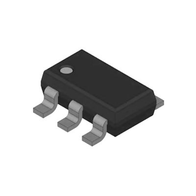
- Use TI's current DBV land pattern and verify pin-1 orientation.
- Place IN and OUT capacitors close to their pins with short ground returns.
- Keep the enable trace at a defined logic level and away from noisy switching nodes.
- Calculate junction temperature from actual dissipation and board conditions.
The registered JPG exists locally, returned HTTP 200 as JPEG in production, and was visually checked as a five-lead SOT-23 illustration.
Pin Functions
The following assignment applies to the DBV 5-pin SOT-23 top view.
Key Specifications
| Manufacturer | Texas Instruments |
|---|---|
| Regulator type | Fixed-output low-dropout linear regulator |
| Output voltage | 1.8 V nominal |
| Input operating range | 1.6 V to 6.0 V |
| Output current | Up to 300 mA |
| Output tolerance | +/-40 mV maximum under the stated DBV conditions for outputs below 2.8 V |
| Dropout voltage | 205 mV maximum at 300 mA for the DBV package and 1.5 V to below 2.5 V outputs |
| Ground current | 6.5 microamperes typical at no load; 15 microamperes maximum over -40 to +125 degrees C |
| Shutdown current | 0.07 microamperes typical, 0.2 microamperes maximum at 25 degrees C |
| PSRR | 95 dB typical at 1 kHz and 20 mA; 92 dB typical at 1 kHz and 300 mA |
| Output discharge | 150 ohms typical when disabled |
| Start-up time | 750 microseconds typical, 1150 microseconds maximum |
| Operating junction temperature | -40 degrees C to +125 degrees C |
| Thermal resistance | 187.1 degrees C/W junction-to-ambient for the DBV JEDEC test condition |
| Package and media | 5-pin SOT-23 (DBV), 3,000-piece large tape-and-reel |
Values apply only under their stated data-sheet test conditions. Validate headroom, transient response, and temperature in the final design.
Replacement Considerations
A candidate replacement must match the fixed 1.8 V output, 300 mA requirement, SOT-23-5 footprint and pin order, input range, enable thresholds, smart pull-down behavior, active output discharge, capacitor stability, dropout, PSRR, noise, and thermal limits. Similar TPS7A20 voltage or package options are not unconditional substitutes.
No internal replacement link is asserted without an exact catalog match and circuit-level review.
Manufacturer Information
Texas Instruments lists TPS7A2018PDBVR as an active 300 mA ultra-low-noise, low-IQ, high-PSRR LDO. In the order code, 18 identifies the fixed 1.8 V output, P denotes active discharge, DBV identifies the 5-pin SOT-23 package, and R denotes the 3,000-piece large tape-and-reel option.
Applications
RF and analog rails
Low noise and high PSRR support sensitive signal-chain circuits.
Network cameras
Compact 1.8 V regulation can supply imaging and communications subsystems.
Portable medical equipment
Low quiescent current supports battery-powered instruments.
Wearables and smart meters
The small SOT-23 package and ceramic-capacitor operation reduce solution area.
Quality & Authenticity
Confirm the full TPS7A2018PDBVR order code, reel label, top marking, pin-1 indicator, five-pin DBV dimensions, and lot traceability during incoming inspection. Package appearance alone does not establish identity or authenticity. Electrical checks should follow the latest TI limits and conditions.
FAQ
What output does TPS7A2018PDBVR provide?
It provides a fixed 1.8 V output at loads up to 300 mA, subject to dropout and thermal limits.
Can EN be left floating?
Yes. The smart enable circuit connects an internal pull-down when EN is not asserted, holding the device off.
Does this option discharge the output?
Yes. The P-version order code includes active output discharge, specified as 150 ohms typical when disabled.
What output capacitor is required?
Use at least 1 microfarad effective ceramic output capacitance within the data-sheet ESR and capacitance limits.
Which package is used?
The DBV suffix identifies TI's 5-pin SOT-23 package, represented by the registered SOT-753 image.
Engineering Notice
Validate input headroom, line and load transients, capacitor bias derating, enable thresholds, output-discharge timing, and junction temperature on the final PCB. Do not rely on active discharge to remove a large output charge after VIN collapses; TI limits reverse current and requires system-level evaluation.
TPS7A2018PDBVR Information
- Specifications
- Tags
- Product attributes
- Attribute value
- Manufacturer:
- Texas Instruments
- Series:
- -
- Package/Case:
- SC-74A, SOT-753
- Packaging:
- Tape & Reel (TR)
- Product Status:
- Active
- Output Configuration:
- Positive
- Output Type:
- Fixed
- Number of Regulators:
- 1
- Voltage - Input (Max):
- 6V
- Voltage - Output (Min/Fixed):
- 1.8V
- Voltage - Output (Max):
- -
- Voltage Dropout (Max):
- 0.2V @ 300mA
- Current - Output:
- 300mA
- Current - Quiescent (Iq):
- 15 µA
- Current - Supply (Max):
- 2 mA
- PSRR:
- 65dB ~ 40dB (100Hz ~ 1MHz)
- Control Features:
- Enable
- Protection Features:
- Over Current, Over Temperature, Under Voltage Lockout (UVLO)
- Operating Temperature:
- -40°C ~ 125°C (TJ)
- Grade:
- -
- Qualification:
- -
- Mounting Type:
- Surface Mount
- Supplier Device Package:
- SOT-23-5
- Include Parts
- Popular Search
The following parts include "TPS7A2018PDBVR" in Silicon Labs TPS7A2018PDBVR.
- Part Number
- Manufacturer
- Package
- Description
- MIC5504-1.8YM5-TR Microchip Technology SC-74A, SOT-753 IC REG LINEAR 1.8V 300MA SOT23-5
- MIC5504-3.3YM5-TR Microchip Technology SC-74A, SOT-753 IC REG LINEAR 3.3V 300MA SOT23-5
- MIC5365-3.0YC5-TR Microchip Technology 5-TSSOP, SC-70-5, SOT-353 IC REG LINEAR 3V 150MA SC70-5
- MIC5365-1.8YC5-TR Microchip Technology 5-TSSOP, SC-70-5, SOT-353 IC REG LINEAR 1.8V 150MA SC70-5
- MIC5365-2.5YC5-TR Microchip Technology 5-TSSOP, SC-70-5, SOT-353 IC REG LINEAR 2.5V 150MA SC70-5
- MIC5365-3.3YC5-TR Microchip Technology 5-TSSOP, SC-70-5, SOT-353 IC REG LINEAR 3.3V 150MA SC70-5
- MIC5365-3.3YD5-TR Microchip Technology SOT-23-5 Thin, TSOT-23-5 IC REG LIN 3.3V 150MA TSOT23-5
- MIC5317-3.3YM5-TR Microchip Technology SC-74A, SOT-753 IC REG LINEAR 3.3V 150MA SOT23-5
- TLV1117LV33DCYR Texas Instruments TO-261-4, TO-261AA IC REG LINEAR 3.3V 1A SOT223-4
- MIC5317-3.3YMT-TZ Microchip Technology 4-UDFN Exposed Pad IC REG LINEAR 3.3V 150MA 4DFN
The following parts are popular search parts in Test and Measurement.
Inventory:7,906
Please send an inquiry. Send us your inquiry, and we will respond immediately.


