 Hello! now
 tms@lcdchip.com



Texas Instruments LM317LIDR
- Part No.:
- LM317LIDR
- Manufacturer:
- Texas Instruments
- Package:
- 8-SOIC (0.154", 3.90mm Width)
- Description:
- IC REG LIN POS ADJ 100MA 8SOIC
- Quantity:
Unit Price:$0
Ext Price:$0
- Payment:

- Shipping:


Product Details
LM317LIDR - 100 mA Adjustable Positive Regulator
Texas Instruments LM317LIDR is an adjustable three-terminal positive linear regulator for 1.25 V to 37 V outputs and load currents up to 100 mA, supplied in an 8-pin SOIC tape-and-reel package.
Electrical, pin, package, and ordering details were checked against TI data sheet SLCS144G and the exact LM317LIDR manufacturer page.
Overview
The LM317LIDR uses two external resistors to set a positive output from 1.25 V to 37 V. Its floating architecture responds to the input-to-output differential rather than ground-referenced input voltage. Internal current limiting and thermal overload protection support low-current adjustable rails, precision current sources, and tracking supplies.
Key Advantages
Adjustable output
Two resistors program output voltage across the supported 1.25 V to 37 V range.
Floating operation
The regulator operates from the input-to-output differential, enabling high-side uses within rated limits.
No mandatory output capacitor
An output capacitor is not required for basic stability, although it can improve transient response.
Integrated protection
Current limiting and thermal overload protection reduce external protection complexity.
Feature Summary
Up to 100 mA
Supplies regulated output current from the specified minimum load through 100 mA.
Precision reference
The output-to-adjustment reference is approximately 1.25 V under specified conditions.
Ripple rejection
An adjustment-pin bypass capacitor can substantially improve 120 Hz rejection.
Industrial temperature
The LM317LI grade is specified from -40 degrees C to +125 degrees C junction temperature.
Package & Footprint
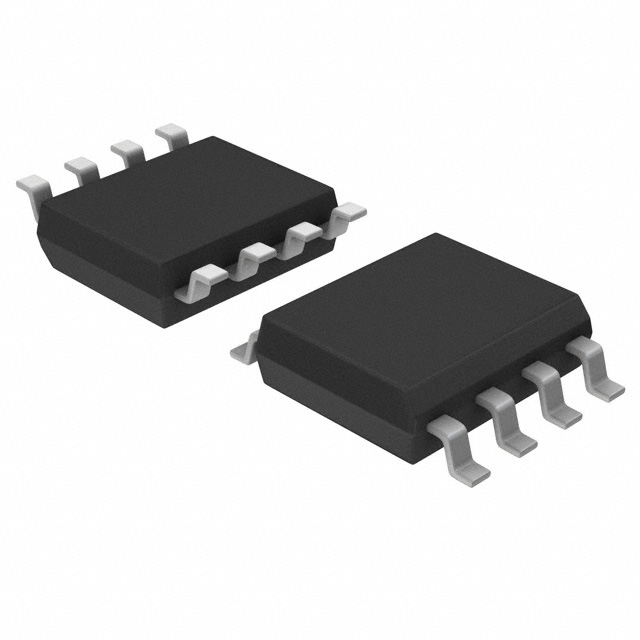
TI identifies D as an 8-pin SOIC. The catalog records it as 8-SOIC (0.154 inch, 3.90 mm body width), and the existing registry image is used.

- Use TI's current D-package land pattern and verify pin-1 orientation.
- Connect every OUTPUT pin to the regulated-output copper.
- Keep the feedback divider close to OUTPUT and ADJUSTMENT.
- Grounding NC pins can improve thermal performance but is not mandatory.
The registered JPG exists locally, returned HTTP 200 as JPEG in production, and was visually checked as an eight-lead SOIC illustration.
Pin Functions
The assignment below applies to the D-package top view.
Key Specifications
| Manufacturer | Texas Instruments |
|---|---|
| Regulator type | Adjustable positive linear regulator |
| Output-voltage range | 1.25 V to 37 V |
| Recommended differential | 2.5 V to 37 V from INPUT to OUTPUT |
| Output-current range | 2.5 mA to 100 mA |
| Reference voltage | Approximately 1.25 V from OUTPUT to ADJUSTMENT; exact limits depend on chip revision |
| Typical dropout | Approximately 2 V |
| Typical line regulation | As low as 0.007% per volt for the new chip under stated conditions |
| Output regulation | 25 mV at 25 degrees C for outputs at or below 5 V under stated conditions |
| Ripple rejection | 55 dB minimum without adjustment bypass; up to 71.5 dB typical for the new chip with bypass at 120 Hz |
| Output noise | 10 microvolts per volt, 10 Hz to 10 kHz, typical |
| Adjustment current | 44 microamperes typical, 57 microamperes maximum for the new chip |
| Operating junction temperature | -40 degrees C to +125 degrees C |
| SOIC thermal resistance | Approximately 96.5 to 98.18 degrees C/W junction-to-ambient depending on chip revision |
| Package and media | 8-pin SOIC (D), 2,500-piece large tape-and-reel |
TI supplies legacy and new chip revisions under this orderable part. Use the applicable data-sheet limits and quality information for the received lot.
Replacement Considerations
A candidate replacement must match the adjustable range, 100 mA requirement, allowed differential, minimum load, D-package footprint, unusual multiple-OUTPUT pin map, reference behavior, adjustment current, protection, and thermal limits. Standard three-pin LM317 variants are not footprint-compatible with this SOIC assignment.
No internal replacement link is asserted without an exact API-confirmed catalog match and engineering review.
Manufacturer Information
Texas Instruments lists LM317LIDR as active. LM317L identifies the 100 mA adjustable regulator family, I identifies the -40 degrees C to +125 degrees C grade, D identifies the 8-pin SOIC, and R identifies the 2,500-piece large tape-and-reel option. TI quality data lists device marking L317LI.
Applications
Adjustable local rails
Generate a board-level voltage selected by two external resistors.
Precision current sources
Use the reference voltage with a programming resistor to establish a controlled current.
Tracking regulators
Build positive supplies that follow a reference or companion rail.
Post-regulation
Reduce ripple after a preregulator when differential voltage and dissipation are controlled.
Quality & Authenticity
Confirm the exact LM317LIDR order code, L317LI marking, reel label, SOIC dimensions, pin-1 indicator, and lot traceability during incoming inspection. Package appearance alone does not establish authenticity. Electrical verification must account for the applicable TI chip revision.
FAQ
How is the output voltage set?
Use two external resistors between OUTPUT, ADJUSTMENT, and ground according to TI's design equation.
Is an output capacitor required?
No capacitor is required for basic stability, but an output capacitor can improve transient response.
Why are there four OUTPUT pins?
Pins 2, 3, 6, and 7 are internally connected and must be treated as the common regulated-output node.
What minimum load is required?
The recommended operating range begins at 2.5 mA; verify the applicable revision-specific regulation conditions.
Can it supply more than 100 mA?
No. Design to the 100 mA recommended maximum and the package thermal limit.
Engineering Notice
Validate differential voltage, programmed output, minimum load, current limit, capacitor placement, protection diodes for stored-energy nodes, and junction temperature in the final circuit. Power dissipation is approximately (VIN minus VOUT) multiplied by load current plus bias effects.
LM317LIDR Information
- Specifications
- Tags
- Product attributes
- Attribute value
- Manufacturer:
- Texas Instruments
- Series:
- -
- Package/Case:
- 8-SOIC (0.154", 3.90mm Width)
- Packaging:
- Tape & Reel (TR)
- Product Status:
- Active
- Output Configuration:
- Positive
- Output Type:
- Adjustable
- Number of Regulators:
- 1
- Voltage - Input (Max):
- 38V
- Voltage - Output (Min/Fixed):
- 1.2V
- Voltage - Output (Max):
- 32V
- Voltage Dropout (Max):
- -
- Current - Output:
- 100mA
- Current - Quiescent (Iq):
- 2.5 mA
- Current - Supply (Max):
- -
- PSRR:
- 80dB ~ 65dB (120Hz)
- Control Features:
- -
- Protection Features:
- Over Current, Over Temperature, Short Circuit
- Operating Temperature:
- -40°C ~ 125°C
- Grade:
- -
- Qualification:
- -
- Mounting Type:
- Surface Mount
- Supplier Device Package:
- 8-SOIC
- Include Parts
- Popular Search
The following parts include "LM317LIDR" in Silicon Labs LM317LIDR.
- Part Number
- Manufacturer
- Package
- Description
- MIC5504-1.8YM5-TR Microchip Technology SC-74A, SOT-753 IC REG LINEAR 1.8V 300MA SOT23-5
- MIC5504-3.3YM5-TR Microchip Technology SC-74A, SOT-753 IC REG LINEAR 3.3V 300MA SOT23-5
- MIC5365-3.0YC5-TR Microchip Technology 5-TSSOP, SC-70-5, SOT-353 IC REG LINEAR 3V 150MA SC70-5
- MIC5365-1.8YC5-TR Microchip Technology 5-TSSOP, SC-70-5, SOT-353 IC REG LINEAR 1.8V 150MA SC70-5
- MIC5365-2.5YC5-TR Microchip Technology 5-TSSOP, SC-70-5, SOT-353 IC REG LINEAR 2.5V 150MA SC70-5
- MIC5365-3.3YC5-TR Microchip Technology 5-TSSOP, SC-70-5, SOT-353 IC REG LINEAR 3.3V 150MA SC70-5
- MIC5365-3.3YD5-TR Microchip Technology SOT-23-5 Thin, TSOT-23-5 IC REG LIN 3.3V 150MA TSOT23-5
- MIC5317-3.3YM5-TR Microchip Technology SC-74A, SOT-753 IC REG LINEAR 3.3V 150MA SOT23-5
- TLV1117LV33DCYR Texas Instruments TO-261-4, TO-261AA IC REG LINEAR 3.3V 1A SOT223-4
- MIC5317-3.3YMT-TZ Microchip Technology 4-UDFN Exposed Pad IC REG LINEAR 3.3V 150MA 4DFN
The following parts are popular search parts in Test and Measurement.
Inventory:7,165
Please send an inquiry. Send us your inquiry, and we will respond immediately.


