 Hello! now
 tms@lcdchip.com



Texas Instruments LM317LCDR
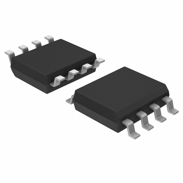
- Part No.:
- LM317LCDR
- Manufacturer:
- Texas Instruments
- Package:
- 8-SOIC (0.154", 3.90mm Width)
- Description:
- IC REG LIN POS ADJ 100MA 8SOIC
- Quantity:
Unit Price:$0
Ext Price:$0
- Payment:

- Shipping:


Product Details
LM317LCDR - 100 mA Adjustable Positive Linear Regulator
Texas Instruments LM317LCDR is an adjustable three-terminal positive linear regulator for 1.25 V to 37 V output applications, supplied in an 8-pin SOIC D package.
Electrical limits, pin functions, package details, and orderable status were checked against the official TI LM317L datasheet and exact part-detail page.
Overview
LM317LCDR provides an adjustable positive output using two external resistors and can deliver up to 100 mA when input headroom and thermal conditions are satisfied. Internal current limiting and thermal-overload protection help protect the regulator under abnormal operating conditions.
Key Advantages
Adjustable output
Two resistors set the regulated output above the approximately 1.25 V reference.
Useful voltage span
The current TI design supports regulated outputs from 1.25 V to 37 V when operating limits are observed.
Integrated protection
Current limiting and thermal-overload protection are built into the regulator.
Stable basic design
An output capacitor is not required for stability, though capacitors can improve transient and ripple performance.
Feature Summary
100 mA regulator
Designed for loads up to 100 mA subject to differential voltage and thermal limits.
Floating regulation
The control circuit operates relative to the output, allowing regulation at elevated output voltages.
Low adjustment current
Adjustment-pin current is 50 microamps typical and 100 microamps maximum under the stated conditions.
SOIC implementation
The D package provides duplicated output leads that are internally connected.
Package & Footprint
TI specifies LM317LCDR in the 8-pin SOIC D package. The catalog designation is 8-SOIC with a nominal 0.154-inch, 3.90 mm body width. TI gives a nominal package size of approximately 4.9 mm by 6.0 mm.

- Use the current TI D-package drawing for land-pattern dimensions.
- Observe top-view pin numbering and the pin-1 indicator.
- Connect all four OUTPUT pins as required by the schematic and footprint.
- Keep the adjustment network close to the device and use short returns.
The registered JPG is checked locally and at the production URL before publication.
Pin Functions
The 8-pin SOIC D assignment follows the official TI top-view diagram.
Do not assume another 8-pin regulator has the same duplicated-output arrangement.
Key Specifications
| Manufacturer | Texas Instruments |
|---|---|
| Regulator type | Adjustable positive linear regulator |
| Output range | 1.25 V to 37 V for the current TI design |
| Output current | Up to 100 mA, subject to operating conditions |
| Reference voltage | 1.20 V minimum, 1.25 V typical, 1.30 V maximum |
| Recommended input-to-output differential | 2.5 V to 37 V for the current TI design |
| Adjustment-pin current | 50 microamps typical, 100 microamps maximum |
| Input regulation | 0.01 percent per volt typical; 0.02 percent per volt maximum at 25 degrees C under the stated condition |
| Ripple rejection | 65 dB minimum under the stated test condition; an adjustment bypass capacitor can improve rejection |
| Output noise | 30 microvolts per volt of output, typical, over the stated bandwidth |
| Protection | Internal current limiting and thermal-overload protection |
| Exact-orderable temperature listing | 0 degrees C to +125 degrees C |
| Package | 8-pin SOIC D, approximately 4.9 mm by 6.0 mm |
| Lead finish and sensitivity | RoHS and REACH compliant; moisture sensitivity level 1 at 260 degrees C |
| Orderable form | Large tape and reel, 2500 pieces; device marking L317LC |
Typical values are not guaranteed limits. Apply the conditions, revision notes, derating curves, and absolute maximum ratings in the current TI documentation.
Replacement Considerations
A replacement must match the adjustable positive-regulator topology, reference range, 100 mA load requirement, allowable input-to-output differential, operating temperature, protection behavior, SOIC footprint, and unusual duplicated OUTPUT pins. Confirm whether legacy or current-silicon voltage limits apply to the intended design.
No internal replacement link is asserted without an exact API-confirmed catalog match and engineering review.
Manufacturer Information
Texas Instruments lists LM317LCDR as an active product. The exact orderable uses the 8-pin SOIC D package, has an official temperature listing of 0 degrees C to +125 degrees C, ships in 2500-piece large tape and reel, and carries the L317LC marking.
Applications
Adjustable local rails
Create a low-current regulated rail using a two-resistor setting network.
Post-regulation
Reduce ripple after a higher-voltage supply when headroom and dissipation allow.
Constant-current circuits
Use the reference voltage with an appropriate resistor in supported current-regulator configurations.
Laboratory and control circuits
Provide a simple adjustable bias or auxiliary supply within the electrical and thermal limits.
Quality & Authenticity
Verify the complete LM317LCDR order code, L317LC marking, SOIC body and lead dimensions, reel label, moisture-sensitivity information, lead finish, and lot traceability during incoming inspection. Package appearance alone does not establish authenticity.
FAQ
What output voltage can LM317LCDR provide?
The current TI design supports adjustment from 1.25 V to 37 V when headroom and other operating limits are met.
How is the output voltage set?
A resistor from OUTPUT to ADJUSTMENT and a second resistor from ADJUSTMENT to the return establish the output voltage.
Is an output capacitor required?
No output capacitor is required for basic stability, but capacitors can improve transient response and ripple rejection.
Why are there four OUTPUT pins?
Pins 2, 3, 6, and 7 are internally connected to the regulator output in the TI D package.
Can every LM317L variant replace this device?
No. Confirm package, pinout, temperature range, voltage limits, protection behavior, and orderable suffix before substitution.
Engineering Notice
Check worst-case input headroom, minimum load behavior, resistor tolerances, adjustment current error, output-current capability, junction temperature, and power dissipation across the full operating envelope. Consult the current TI documentation when designing with legacy or current silicon revisions.
LM317LCDR Information
- Specifications
- Tags
- Product attributes
- Attribute value
- Manufacturer:
- Texas Instruments
- Series:
- -
- Package/Case:
- 8-SOIC (0.154", 3.90mm Width)
- Packaging:
- Tape & Reel (TR)
- Product Status:
- Active
- Output Configuration:
- Positive
- Output Type:
- Adjustable
- Number of Regulators:
- 1
- Voltage - Input (Max):
- 38V
- Voltage - Output (Min/Fixed):
- 1.2V
- Voltage - Output (Max):
- 32V
- Voltage Dropout (Max):
- -
- Current - Output:
- 100mA
- Current - Quiescent (Iq):
- 2.5 mA
- Current - Supply (Max):
- -
- PSRR:
- 80dB ~ 65dB (120Hz)
- Control Features:
- -
- Protection Features:
- Over Current, Over Temperature, Short Circuit
- Operating Temperature:
- 0°C ~ 125°C
- Grade:
- -
- Qualification:
- -
- Mounting Type:
- Surface Mount
- Supplier Device Package:
- 8-SOIC
- Include Parts
- Popular Search
The following parts include "LM317LCDR" in Silicon Labs LM317LCDR.
- Part Number
- Manufacturer
- Package
- Description
- MIC5504-1.8YM5-TR Microchip Technology SC-74A, SOT-753 IC REG LINEAR 1.8V 300MA SOT23-5
- MIC5504-3.3YM5-TR Microchip Technology SC-74A, SOT-753 IC REG LINEAR 3.3V 300MA SOT23-5
- MIC5365-3.0YC5-TR Microchip Technology 5-TSSOP, SC-70-5, SOT-353 IC REG LINEAR 3V 150MA SC70-5
- MIC5365-1.8YC5-TR Microchip Technology 5-TSSOP, SC-70-5, SOT-353 IC REG LINEAR 1.8V 150MA SC70-5
- MIC5365-2.5YC5-TR Microchip Technology 5-TSSOP, SC-70-5, SOT-353 IC REG LINEAR 2.5V 150MA SC70-5
- MIC5365-3.3YC5-TR Microchip Technology 5-TSSOP, SC-70-5, SOT-353 IC REG LINEAR 3.3V 150MA SC70-5
- MIC5365-3.3YD5-TR Microchip Technology SOT-23-5 Thin, TSOT-23-5 IC REG LIN 3.3V 150MA TSOT23-5
- MIC5317-3.3YM5-TR Microchip Technology SC-74A, SOT-753 IC REG LINEAR 3.3V 150MA SOT23-5
- TLV1117LV33DCYR Texas Instruments TO-261-4, TO-261AA IC REG LINEAR 3.3V 1A SOT223-4
- MIC5317-3.3YMT-TZ Microchip Technology 4-UDFN Exposed Pad IC REG LINEAR 3.3V 150MA 4DFN
The following parts are popular search parts in Test and Measurement.
Inventory:6,206
Please send an inquiry. Send us your inquiry, and we will respond immediately.


